5T9070PAGI
Obsolete1-TO-10 LVCMOS/LVTTL FANOUT BUFFER
Deep-Dive with AI
Search across all available documentation for this part.
5T9070PAGI
Obsolete1-TO-10 LVCMOS/LVTTL FANOUT BUFFER
Deep-Dive with AI
Technical Specifications
Parameters and characteristics for this part
| Specification | 5T9070PAGI |
|---|---|
| Differential - Input:Output | False |
| Frequency - Max [Max] | 200 MHz |
| Mounting Type | Surface Mount |
| Number of Circuits | 1 |
| Operating Temperature [Max] | 85 °C |
| Operating Temperature [Min] | -40 °C |
| Output | LVTTL |
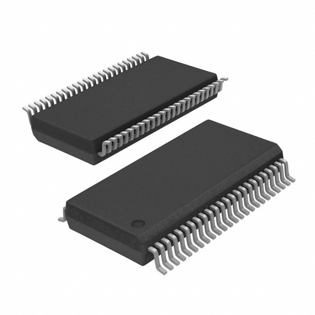
| Package / Case | 48-TFSOP |
| Package / Case | 0.24 in |
| Package / Case [custom] | 6.1 mm |
| Ratio - Input:Output [custom] | 1:10 |
| Supplier Device Package | 48-TSSOP |
| Type | Fanout Buffer (Distribution) |
| Voltage - Supply [Max] | 2.7 V |
| Voltage - Supply [Min] | 2.3 V |
Pricing
Prices provided here are for design reference only. For realtime values and availability, please visit the distributors directly
| Distributor | Package | Quantity | $ | |
|---|---|---|---|---|
Description
General part information
5T9070 Series
The 5T9070 2.5V single data rate (SDR) clock buffer is a single-ended input to ten single-ended outputs buffer built on advanced metal CMOS technology. The SDR clock buffer fanout from a single input to ten single-ended outputs reduces the loading on the preceding driver and provides an efficient clock distribution network. The 5T9070 has two output banks that can be asynchronously enabled/ disabled. Multiple power and grounds reduce noise.
Documents
Technical documentation and resources