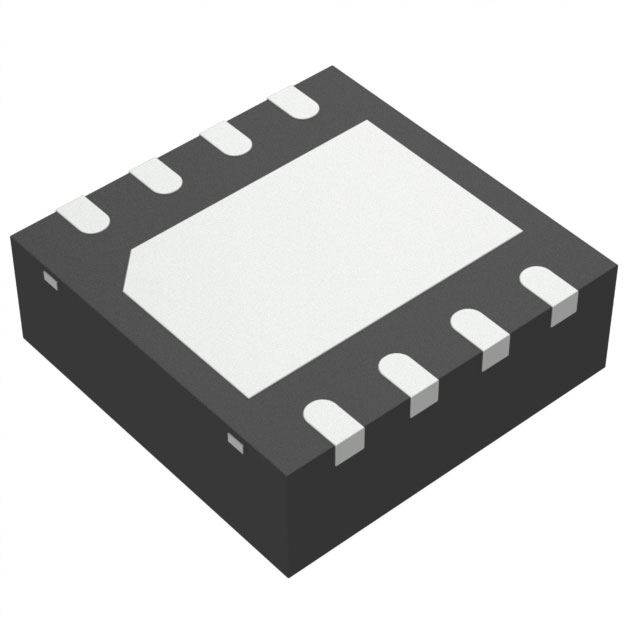
UCC27211ADRMR
Active4-A, 120-V HALF BRIDGE GATE DRIVER WITH 8-V UVLO AND NEGATIVE VOLTAGE HANDLING
Deep-Dive with AI
Search across all available documentation for this part.

UCC27211ADRMR
Active4-A, 120-V HALF BRIDGE GATE DRIVER WITH 8-V UVLO AND NEGATIVE VOLTAGE HANDLING
Technical Specifications
Parameters and characteristics for this part
| Specification | UCC27211ADRMR |
|---|---|
| Channel Type | Independent |
| Current - Peak Output (Source, Sink) [custom] | 4 A |
| Current - Peak Output (Source, Sink) [custom] | 4 A |
| Driven Configuration | Half-Bridge |
| Gate Type | N-Channel MOSFET |
| High Side Voltage - Max (Bootstrap) [Max] | 120 V |
| Input Type | Non-Inverting |
| Logic Voltage - VIL, VIH | 1.3 V, 2.7 V |
| Mounting Type | Surface Mount |
| Number of Drivers | 2 |
| Operating Temperature [Max] | 140 °C |
| Operating Temperature [Min] | -40 °C |
| Package / Case | 8-VDFN Exposed Pad |
| Rise / Fall Time (Typ) [custom] | 7.2 ns |
| Rise / Fall Time (Typ) [custom] | 5.5 ns |
| Supplier Device Package | 8-VSON (4x4) |
| Voltage - Supply [Max] | 17 V |
| Voltage - Supply [Min] | 8 V |
Pricing
Prices provided here are for design reference only. For realtime values and availability, please visit the distributors directly
| Distributor | Package | Quantity | $ | |
|---|---|---|---|---|
| Digikey | Cut Tape (CT) | 1 | $ 1.98 | |
| 10 | $ 1.77 | |||
| 25 | $ 1.67 | |||
| 100 | $ 1.43 | |||
| 250 | $ 1.34 | |||
| 500 | $ 1.17 | |||
| 1000 | $ 0.97 | |||
| Digi-Reel® | 1 | $ 1.98 | ||
| 10 | $ 1.77 | |||
| 25 | $ 1.67 | |||
| 100 | $ 1.43 | |||
| 250 | $ 1.34 | |||
| 500 | $ 1.17 | |||
| 1000 | $ 0.97 | |||
| Tape & Reel (TR) | 3000 | $ 0.71 | ||
| 6000 | $ 0.68 | |||
| 15000 | $ 0.66 | |||
| Texas Instruments | LARGE T&R | 1 | $ 1.55 | |
| 100 | $ 1.28 | |||
| 250 | $ 0.92 | |||
| 1000 | $ 0.69 | |||
Description
General part information
UCC27211A-Q1 Series
The UCC27211A-Q1 device driver is based on the popular UCC27201 MOSFET drivers; but, this device offers several significant performance improvements.
The peak output pullup and pulldown current has been increased to 3.7A source and 4.5A sink and thereby allows for driving large power MOSFETs with minimized switching losses during the transition through the Miller Plateau of the MOSFET. The input structure can directly handle –10VDC, which increases robustness and also allows direct interface to gate-drive transformers without using rectification diodes. The inputs are also independent of supply voltage and have a 20V maximum rating.
The switching node of the UCC27211A-Q1 (HS pin) can handle –(24 - VDD) V maximum, which allows the high-side channel to be protected from inherent negative voltages caused by parasitic inductance and stray capacitance. The UCC27211A-Q1 (TTL inputs) has increased hysteresis that allows for interface to analog or digital PWM controllers with enhanced noise immunity.
Documents
Technical documentation and resources


