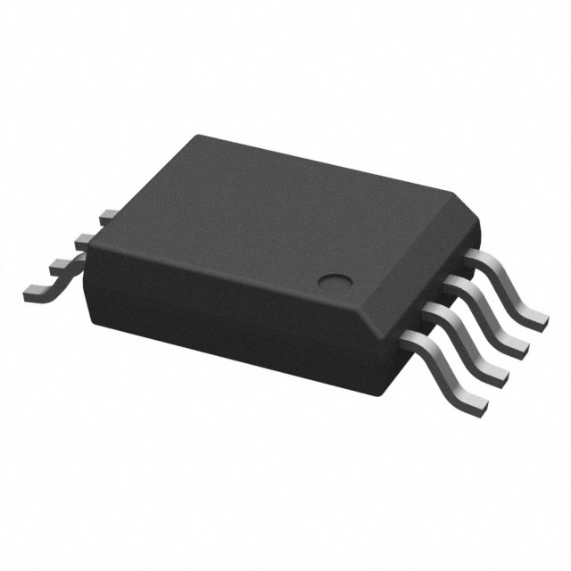
UCC5350MCQDWVQ1
AUTOMOTIVE ±5A SINGLE-CHANNEL ISOLATED GATE DRIVER WITH MILLER CLAMP OR SPLIT OUTPUTS FOR SIC/IGBT
Deep-Dive with AI
Search across all available documentation for this part.

UCC5350MCQDWVQ1
AUTOMOTIVE ±5A SINGLE-CHANNEL ISOLATED GATE DRIVER WITH MILLER CLAMP OR SPLIT OUTPUTS FOR SIC/IGBT
Deep-Dive with AI
Technical Specifications
Parameters and characteristics for this part
| Specification | UCC5350MCQDWVQ1 |
|---|---|
| Approval Agency | CQC, VDE, UL |
| Common Mode Transient Immunity (Min) [Min] | 100 V/ns |
| Current - Output High, Low [custom] | 5 A |
| Current - Output High, Low [custom] | 5 A |
| Current - Peak Output | 5 A |
| Grade | Automotive |
| Mounting Type | Surface Mount |
| Number of Channels | 1 |
| Operating Temperature [Max] | 125 °C |
| Operating Temperature [Min] | -40 °C |
| Package / Case | 8-SOIC |
| Package / Case [custom] | 0.295 in |
| Package / Case [custom] | 7.5 mm |
| Propagation Delay tpLH / tpHL (Max) [custom] | 100 ns |
| Propagation Delay tpLH / tpHL (Max) [custom] | 100 ns |
| Pulse Width Distortion (Max) [Max] | 20 ns |
| Qualification | AEC-Q100 |
| Rise / Fall Time (Typ) [custom] | 10 ns |
| Rise / Fall Time (Typ) [custom] | 10 ns |
| Supplier Device Package | 8-SOIC |
| Technology | Capacitive Coupling |
| Voltage - Output Supply [Max] | 33 V |
| Voltage - Output Supply [Min] | 13.2 V |
Pricing
Prices provided here are for design reference only. For realtime values and availability, please visit the distributors directly
| Distributor | Package | Quantity | $ | |
|---|---|---|---|---|
| Digikey | Tube | 1 | $ 5.39 | |
| 10 | $ 3.61 | |||
| 25 | $ 3.15 | |||
| 100 | $ 2.63 | |||
| 250 | $ 2.38 | |||
| 500 | $ 2.23 | |||
| Texas Instruments | TUBE | 1 | $ 3.76 | |
| 100 | $ 3.10 | |||
| 250 | $ 2.23 | |||
| 1000 | $ 1.68 | |||
Description
General part information
UCC5350-Q1 Series
The UCC5350-Q1 is a single-channel, isolated gate driver with 10A source and 10A sink typical peak current designed to drive MOSFETs, IGBTs, and SiC MOSFETs. The UCC5350-Q1 has the option for Miller clamp or Split Outputs. The CLAMP pin is used to connect the transistor gate to an internal FET beside the output to prevent false turn-on caused by Miller current injection. The split outputs option allows separate control of the rise and fall times of the gate voltage with OUTH and OUTL pins.
The UCC5350-Q1 is available in a 4mm SOIC-8 (D) or 8.5mm wide body SOIC-8 (DWV) package and can support isolation voltage up to 3kVRMS and 5kVRMS, respectively. The input side is isolated from the output side with SiO2 capacitive isolation technology with longer than 40 years isolation barrier lifetime. The UCC5350-Q1 is a good fit for driving IGBTs or MOSFETs in applications such as high-voltage traction inverters and on-board chargers.
Compared to an opto-isolated gate driver, the UCC5350-Q1 device has lower part-to-part skew, lower propagation delay, higher operating temperature, and higher CMTI.
Documents
Technical documentation and resources


