UCC27611DRVR
Active4-A/6-A SINGLE-CHANNEL GATE DRIVER WITH 4-V UVLO AND 5-V REGULATED OUTPUT
Deep-Dive with AI
Search across all available documentation for this part.
UCC27611DRVR
Active4-A/6-A SINGLE-CHANNEL GATE DRIVER WITH 4-V UVLO AND 5-V REGULATED OUTPUT
Technical Specifications
Parameters and characteristics for this part
| Specification | UCC27611DRVR |
|---|---|
| Channel Type | Single |
| Current - Peak Output (Source, Sink) [custom] | 6 A |
| Current - Peak Output (Source, Sink) [custom] | 4 A |
| Driven Configuration | Low-Side |
| Gate Type | N-Channel MOSFET |
| Input Type | Non-Inverting, Inverting |
| Logic Voltage - VIL, VIH | 1.3 V, 1.85 V |
| Mounting Type | Surface Mount |
| Number of Drivers | 1 |
| Operating Temperature [Max] | 140 °C |
| Operating Temperature [Min] | -40 °C |
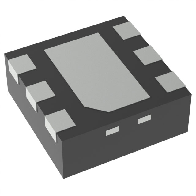
| Supplier Device Package | 6-WSON (2x2) |
| Voltage - Supply [Max] | 18 V |
| Voltage - Supply [Min] | 4 V |
Pricing
Prices provided here are for design reference only. For realtime values and availability, please visit the distributors directly
| Distributor | Package | Quantity | $ | |
|---|---|---|---|---|
| Digikey | Cut Tape (CT) | 1 | $ 1.50 | |
| 10 | $ 1.34 | |||
| 25 | $ 1.27 | |||
| 100 | $ 1.05 | |||
| 250 | $ 0.98 | |||
| 500 | $ 0.86 | |||
| 1000 | $ 0.68 | |||
| Digi-Reel® | 1 | $ 1.50 | ||
| 10 | $ 1.34 | |||
| 25 | $ 1.27 | |||
| 100 | $ 1.05 | |||
| 250 | $ 0.98 | |||
| 500 | $ 0.86 | |||
| 1000 | $ 0.68 | |||
| Tape & Reel (TR) | 3000 | $ 0.64 | ||
| 6000 | $ 0.60 | |||
| 15000 | $ 0.58 | |||
| Texas Instruments | LARGE T&R | 1 | $ 1.11 | |
| 100 | $ 0.85 | |||
| 250 | $ 0.63 | |||
| 1000 | $ 0.45 | |||
Description
General part information
UCC27611 Series
The UCC27611 is a single-channel, high-speed, gate driver optimized for 5-V drive, specifically addressing enhancement mode GaN FETs. The drive voltage VREF is precisely controlled by internal linear regulator to 5 V. The UCC27611 offers asymmetrical rail-to-rail peak current drive capability with 4-A source and 6-A sink. Split output configuration allows individual turnon and turnoff time optimization depending on FET. Package and pinout with minimum parasitic inductances reduce the rise and fall time and limit the ringing. Additionally, the short propagation delay with minimized tolerances and variations allows efficient operation at high frequencies. The 1-Ω and 0.35-Ω resistance boosts immunity to hard switching with high slew rate dV and dt.
The independence from VDD input signal thresholds ensure TTL and CMOS low-voltage logic compatibility. For safety reason, when the input pins are in a floating condition, the internal input pullup and pulldown resistors hold the output LOW. Internal circuitry on VREF pin provides an undervoltage lockout function that holds output LOW until VREF supply voltage is within operating range. UCC27611 is offered in a small 2.00 mm × 2.00 mm SON-6 package (DRV) with exposed thermal and ground pad that improves the package power-handling capability. The UCC27611 operates over wide temperature range from –40°C to 140°C.
The UCC27611 is a single-channel, high-speed, gate driver optimized for 5-V drive, specifically addressing enhancement mode GaN FETs. The drive voltage VREF is precisely controlled by internal linear regulator to 5 V. The UCC27611 offers asymmetrical rail-to-rail peak current drive capability with 4-A source and 6-A sink. Split output configuration allows individual turnon and turnoff time optimization depending on FET. Package and pinout with minimum parasitic inductances reduce the rise and fall time and limit the ringing. Additionally, the short propagation delay with minimized tolerances and variations allows efficient operation at high frequencies. The 1-Ω and 0.35-Ω resistance boosts immunity to hard switching with high slew rate dV and dt.
Documents
Technical documentation and resources