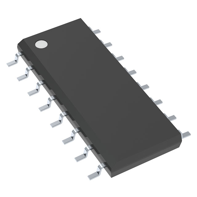
UCC3580DTR-2
Active16V ACTIVE CLAMP CURRENT MODE PWM CONTROLLER WITH P-CHANNEL CLAMP FET AND 10V TURN-ON, 0°C TO 70°C
Deep-Dive with AI
Search across all available documentation for this part.

UCC3580DTR-2
Active16V ACTIVE CLAMP CURRENT MODE PWM CONTROLLER WITH P-CHANNEL CLAMP FET AND 10V TURN-ON, 0°C TO 70°C
Deep-Dive with AI
Technical Specifications
Parameters and characteristics for this part
| Specification | UCC3580DTR-2 |
|---|---|
| Control Features | Soft Start |
| Duty Cycle | 66 % |
| Internal Switch(s) | False |
| Mounting Type | Surface Mount |
| Operating Temperature [Max] | 150 °C |
| Operating Temperature [Min] | -55 °C |
| Output Isolation | Isolated |
| Package / Case | 16-SOIC |
| Package / Case [x] | 0.154 in |
| Package / Case [y] | 3.9 mm |
| Supplier Device Package | 16-SOIC |
| Topology | Flyback, Forward |
| Voltage - Start Up | 15 V |
| Voltage - Supply (Vcc/Vdd) [Max] | 15 V |
| Voltage - Supply (Vcc/Vdd) [Min] | 8.5 V |
Pricing
Prices provided here are for design reference only. For realtime values and availability, please visit the distributors directly
| Distributor | Package | Quantity | $ | |
|---|---|---|---|---|
| Digikey | Tape & Reel (TR) | 2500 | $ 2.36 | |
| Texas Instruments | LARGE T&R | 1 | $ 3.71 | |
| 100 | $ 3.03 | |||
| 250 | $ 2.38 | |||
| 1000 | $ 2.02 | |||
Description
General part information
UCC3580-2 Series
The UCC3580 family of PWM controllers is designed to implement a variety of active clamp/reset and synchronous rectifier switching converter topologies. While containing all the necessary functions for fixed frequency, high performance pulse width modulation, the additional feature of this design is the inclusion of an auxiliary switch driver which complements the main power switch, and with a programmable deadtime or delay between each transition. The active clamp/reset technique allows operation of single ended converters beyond 50% duty cycle while reducing voltage stresses on the switches, and allows a greater flux swing for the power transformer. This approach also allows a reduction in switching losses by recovering energy stored in parasitic elements such as leakage inductance and switch capacitance.
The oscillator is programmed with two resistors and a capacitor to set switching frequency and maximum duty cycle. A separate synchronized ramp provides a voltage feedforward pulse width modulation and a programmed maximum volt-second limit. The generated clock from the oscillator contains both frequency and maximum duty cycle information.
The main gate drive output (OUT1) is controlled by the pulse width modulator. The second output (OUT2) is intended to activate an auxiliary switch during the off time of the main switch, except that between each transition there is deadtime where both switches are off, programmed by a single external resistor. This design offers two options for OUT2, normal and inverted. In the -1 and -2 versions, OUT2 is normal and can be used to drive PMOS FETs. In the -3 and -4 versions, OUT2 is inverted and can be used to drive NMOS FETs. In all versions, both the main and auxiliary switches are held off prior to startup and when the PWM command goes to zero duty cycle. During fault conditions, OUT1 is held off while OUT2 operates at maximum duty cycle with a guaranteed off time equal to the sum of the two deadtimes.
Documents
Technical documentation and resources


