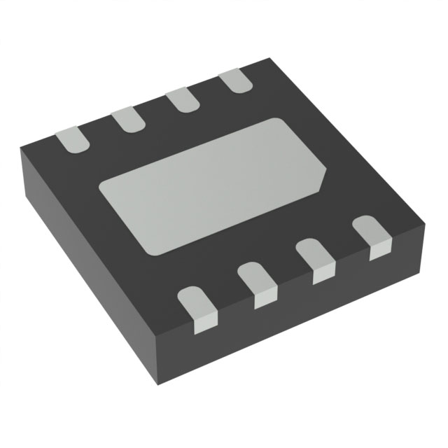
2EDN7524GXTMA1
Active☆ FAST DUAL-CHANNEL 5A GATE DRIVER OPTIMIZED FOR STANDARD + SUPERJUNCTION MOSFETS + GAN POWER SWITCHING DEVICES ☆ SAVES SWITCHING DIODES ☆ PRECISE TIMING
Deep-Dive with AI
Search across all available documentation for this part.

2EDN7524GXTMA1
Active☆ FAST DUAL-CHANNEL 5A GATE DRIVER OPTIMIZED FOR STANDARD + SUPERJUNCTION MOSFETS + GAN POWER SWITCHING DEVICES ☆ SAVES SWITCHING DIODES ☆ PRECISE TIMING
Technical Specifications
Parameters and characteristics for this part
| Specification | 2EDN7524GXTMA1 |
|---|---|
| Channel Type | Independent |
| Current - Peak Output (Source, Sink) [custom] | 5 A |
| Current - Peak Output (Source, Sink) [custom] | 5 A |
| Driven Configuration | Low-Side |
| Gate Type | N-Channel MOSFET |
| Input Type | Non-Inverting |
| Mounting Type | Surface Mount |
| Number of Drivers | 2 |
| Operating Temperature [Max] | 150 °C |
| Operating Temperature [Min] | -40 °C |
| Package / Case | 8-WDFN Exposed Pad |
| Rise / Fall Time (Typ) [custom] | 4.5 ns |
| Rise / Fall Time (Typ) [custom] | 5.3 ns |
| Supplier Device Package | PG-WSON-8-1 |
| Voltage - Supply [Max] | 20 V |
| Voltage - Supply [Min] | 4.5 V |
Pricing
Prices provided here are for design reference only. For realtime values and availability, please visit the distributors directly
| Distributor | Package | Quantity | $ | |
|---|---|---|---|---|
| Digikey | Cut Tape (CT) | 1 | $ 1.62 | |
| 10 | $ 1.45 | |||
| 25 | $ 1.38 | |||
| 100 | $ 1.13 | |||
| 250 | $ 1.06 | |||
| 500 | $ 0.93 | |||
| 1000 | $ 0.74 | |||
| Digi-Reel® | 1 | $ 1.62 | ||
| 10 | $ 1.45 | |||
| 25 | $ 1.38 | |||
| 100 | $ 1.13 | |||
| 250 | $ 1.06 | |||
| 500 | $ 0.93 | |||
| 1000 | $ 0.74 | |||
| Tape & Reel (TR) | 4000 | $ 0.69 | ||
| 8000 | $ 0.65 | |||
| 12000 | $ 0.63 | |||
| Newark | Each (Supplied on Cut Tape) | 1 | $ 0.99 | |
| 10 | $ 0.71 | |||
| 25 | $ 0.64 | |||
| 50 | $ 0.60 | |||
| 100 | $ 0.56 | |||
| 250 | $ 0.53 | |||
| 500 | $ 0.50 | |||
| 1000 | $ 0.49 | |||
Description
General part information
2EDN7524 Series
The input signals are low voltage TTL and 3.3V CMOS-compatible with a very broad voltage handling capability of up to +20V and down to -10VDC. The unique ability to handle -10VDC at the input pins protects the device against ground bouncing. Each of the two outputs is able to sink and source a 5A current utilizing a true rail-to-rail output stage, which ensures very low impedances of 0.7Ω up to the positive and 0.55Ω down to the negativerail respectively. Excellent channel to channel delay matching, typ. 1ns, enables risk-free doubling of the source and sink capability up to 10A peak through paralleling of both channels. The combination of industry standard pin-outs and different logic input/output configurations guarantee high flexibility and shortens R&D time. The gate driver is available in the three package options: PG-DSO-8-pin, PG-VDSON-8-pin and PG-TDSSO-8-pin (small form-factor, improved thermal performance compared to DSO-8).
Documents
Technical documentation and resources


