UCD7232RTJT
ActiveDIGITAL CONTROL COMPATIBLE SYNCHRONOUS-BUCK GATE DRIVER WITH CURRENT SENSE AND FAULT PROTECTION
Deep-Dive with AI
Search across all available documentation for this part.
UCD7232RTJT
ActiveDIGITAL CONTROL COMPATIBLE SYNCHRONOUS-BUCK GATE DRIVER WITH CURRENT SENSE AND FAULT PROTECTION
Deep-Dive with AI
Technical Specifications
Parameters and characteristics for this part
| Specification | UCD7232RTJT |
|---|---|
| Channel Type | Synchronous |
| Current - Peak Output (Source, Sink) [custom] | 4 A |
| Current - Peak Output (Source, Sink) [custom] | 4 A |
| Driven Configuration | Half-Bridge |
| Gate Type | N-Channel MOSFET |
| Input Type | Non-Inverting |
| Logic Voltage - VIL, VIH | 0.8 V, 2 V |
| Mounting Type | Surface Mount |
| Number of Drivers | 2 |
| Operating Temperature [Max] | 125 ¯C |
| Operating Temperature [Min] | -40 °C |
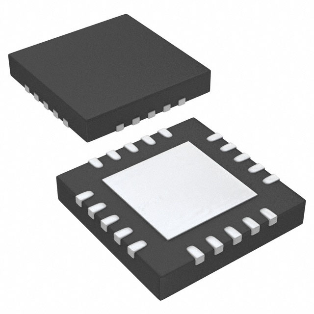
| Package / Case | 20-WFQFN Exposed Pad |
| Rise / Fall Time (Typ) [custom] | 27 ns |
| Rise / Fall Time (Typ) [custom] | 21 ns |
| Supplier Device Package | 20-QFN (4x4) |
| Voltage - Supply [Max] | 15 V |
| Voltage - Supply [Min] | 4.7 V |
Pricing
Prices provided here are for design reference only. For realtime values and availability, please visit the distributors directly
| Distributor | Package | Quantity | $ | |
|---|---|---|---|---|
| Digikey | Cut Tape (CT) | 1 | $ 1.89 | |
| 10 | $ 1.70 | |||
| 25 | $ 1.60 | |||
| 100 | $ 1.36 | |||
| Digi-Reel® | 1 | $ 1.89 | ||
| 10 | $ 1.70 | |||
| 25 | $ 1.60 | |||
| 100 | $ 1.36 | |||
| Tape & Reel (TR) | 250 | $ 0.90 | ||
| 500 | $ 0.79 | |||
| Texas Instruments | SMALL T&R | 1 | $ 1.42 | |
| 100 | $ 1.17 | |||
| 250 | $ 0.84 | |||
| 1000 | $ 0.63 | |||
Description
General part information
UCD7232 Series
The UCD7232 high current driver is specifically designed for digitally-controlled, point-of-load, synchronous buck switching power supplies. Two driver circuits provide high charge and discharge current for the high-side NMOS switch and the low-side NMOS synchronous rectifier in a synchronous buck circuit. The MOSFET gates are driven by an internally regulated VGGsupply. The internal VGGregulator can be disabled to permit the user to supply their own gate drive voltage. This flexibility allows a wide power conversion input voltage range of 2.2 to 15 V. Internal under voltage lockout (UVLO) logic insures VGGis good before allowing chip operation.
A drive logic block allows operation in one of two modes selected by the SRE Mode pin. In Synchronous Mode, the logic block uses the PWM signal to control both the high-side and low-side gate drive signals. Dead time is automatically adjusted to prevent cross conduction. The Synchronous Rectifier Enable (SRE) pin controls whether or not the low-side FET is turned on when the PWM signal is low. In Independent Mode, the PWM and SRE pins control the high-side and low-side gates directly. No anti-cross-conduction logic is used in this mode.
On-board comparators monitor the voltage across the high side switch and the voltage across an external current sense element to safeguard the power stage from sudden high current loads. Blanking delay is set for the high side comparator by a single resistor in order to avoid false reports coincident with switching edge noise. In the event of a high-side fault or an over-current fault, the high-side FET turned off and the Fault Flag (FLT) is asserted to alert the digital controller. The fault thresholds are independently set by the HS Sense and ILIM pins.
Documents
Technical documentation and resources