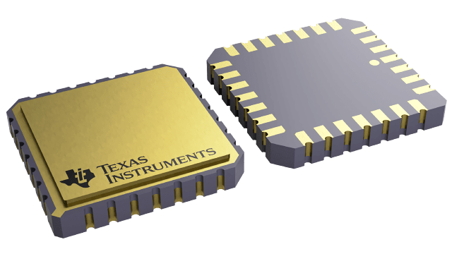
CY54FCT646CTLMB
ActiveOCTAL REGISTERED BUS TRANSCEIVERS WITH 3-STATE OUTPUTS
Deep-Dive with AI
Search across all available documentation for this part.

CY54FCT646CTLMB
ActiveOCTAL REGISTERED BUS TRANSCEIVERS WITH 3-STATE OUTPUTS
Deep-Dive with AI
Technical Specifications
Parameters and characteristics for this part
| Specification | CY54FCT646CTLMB |
|---|---|
| Current - Output High, Low | 12 mA, 48 mA |
| Mounting Type | Surface Mount |
| Number of Bits per Element | 8 |
| Number of Elements | 1 |
| Operating Temperature [Max] | 125 °C |
| Operating Temperature [Min] | -55 °C |
| Output Type | 3-State |
| Package / Case | 28-CLCC |
| Supplier Device Package | 28-LCCC |
| Supplier Device Package [x] | 11.43 |
| Supplier Device Package [y] | 11.43 |
| Voltage - Supply [Max] | 5.5 V |
| Voltage - Supply [Min] | 4.5 V |
Pricing
Prices provided here are for design reference only. For realtime values and availability, please visit the distributors directly
| Distributor | Package | Quantity | $ | |
|---|---|---|---|---|
| Texas Instruments | TUBE | 1 | $ 46.09 | |
| 100 | $ 40.97 | |||
| 250 | $ 33.67 | |||
| 1000 | $ 30.12 | |||
Description
General part information
5962-9222301 Series
The \x92FCT646T devices consist of a bus transceiver circuit with 3-state, D-type flip-flops, and control circuitry arranged for multiplexed transmission of data directly from the input bus or from the internal registers. Data on the A or B bus is clocked into the registers as the appropriate clock pin goes to a high logic level. Output-enable (G\) and direction (DIR) inputs control the transceiver function. In the transceiver mode,data present at the high-impedance port can be stored in either the A or B register, or in both. Select controls (SAB, SBA) can multiplex stored and real-time (transparent mode) data. DIR determines which bus receives data when G\ is low. In the isolation mode (G\ is high), A data can be stored in the B register and/or B data can be stored in the A register.
These devices are fully specified for partial-power-down applications using Ioff. The Ioffcircuitry disables the outputs, preventing damaging current backflow through the device when it is powered down.
The \x92FCT646T devices consist of a bus transceiver circuit with 3-state, D-type flip-flops, and control circuitry arranged for multiplexed transmission of data directly from the input bus or from the internal registers. Data on the A or B bus is clocked into the registers as the appropriate clock pin goes to a high logic level. Output-enable (G\) and direction (DIR) inputs control the transceiver function. In the transceiver mode,data present at the high-impedance port can be stored in either the A or B register, or in both. Select controls (SAB, SBA) can multiplex stored and real-time (transparent mode) data. DIR determines which bus receives data when G\ is low. In the isolation mode (G\ is high), A data can be stored in the B register and/or B data can be stored in the A register.
Documents
Technical documentation and resources


