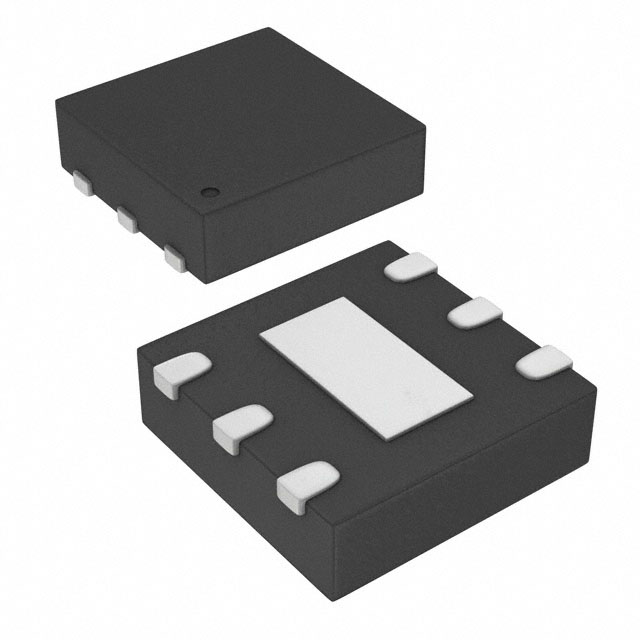
UCC27512MDRSTEP
ActiveENHANCED PRODUCT 4-A/8-A SINGLE-CHANNEL GATE DRIVER WITH 5-V UVLO IN SON PACKAGE
Deep-Dive with AI
Search across all available documentation for this part.

UCC27512MDRSTEP
ActiveENHANCED PRODUCT 4-A/8-A SINGLE-CHANNEL GATE DRIVER WITH 5-V UVLO IN SON PACKAGE
Deep-Dive with AI
Technical Specifications
Parameters and characteristics for this part
| Specification | UCC27512MDRSTEP |
|---|---|
| Channel Type | Single |
| Current - Peak Output (Source, Sink) | 8 A, 4 A |
| Driven Configuration | Low-Side |
| Gate Type | N-Channel MOSFET, IGBT |
| Input Type | Non-Inverting, Inverting |
| Logic Voltage - VIL, VIH [custom] | 1 V |
| Logic Voltage - VIL, VIH [custom] | 2.4 V |
| Mounting Type | Surface Mount |
| Number of Drivers | 1 |
| Operating Temperature [Max] | 125 ¯C |
| Operating Temperature [Min] | -55 °C |
| Rise / Fall Time (Typ) [custom] | 7 ns |
| Rise / Fall Time (Typ) [custom] | 8 ns |
| Supplier Device Package | 6-SON (3x3) |
| Voltage - Supply [Max] | 18 V |
| Voltage - Supply [Min] | 4.5 V |
Pricing
Prices provided here are for design reference only. For realtime values and availability, please visit the distributors directly
| Distributor | Package | Quantity | $ | |
|---|---|---|---|---|
| Digikey | Cut Tape (CT) | 1 | $ 4.26 | |
| 10 | $ 3.83 | |||
| 25 | $ 3.62 | |||
| 100 | $ 3.14 | |||
| Digi-Reel® | 1 | $ 4.26 | ||
| 10 | $ 3.83 | |||
| 25 | $ 3.62 | |||
| 100 | $ 3.14 | |||
| Tape & Reel (TR) | 250 | $ 2.98 | ||
| 500 | $ 2.67 | |||
| 1250 | $ 2.25 | |||
| 2500 | $ 2.14 | |||
| Texas Instruments | SMALL T&R | 1 | $ 3.28 | |
| 100 | $ 2.88 | |||
| 250 | $ 2.02 | |||
| 1000 | $ 1.63 | |||
Description
General part information
UCC27512-EP Series
The UCC27511 and UCC27512 single-channel, high-speed, low-side gate-driver device can effectively drive MOSFET and IGBT power switches. Using a design that inherently minimizes shoot-through current, UCC27511 and UCC27512 are capable of sourcing and sinking high peak-current pulses into capacitive loads offering rail-to-rail drive capability and extremely small propagation delay, typically 13 ns.
UCC27511 features a dual-input design which offers flexibility of implementing both inverting (IN– pin) and noninverting (IN+ pin) configuration with the same device. Either IN+ or IN– pin can be used to control the state of the driver output. The unused input pin can be used for enable and disable functions. For safety purpose, internal pullup and pulldown resistors on the input pins ensure that outputs are held low when input pins are in floating condition. Hence the unused input pin is not left floating and must be properly biased to ensure that driver output is in enabled for normal operation.
The input pin threshold of the UCC27511 device is based on TTL and CMOS-compatible low-voltage logic which is fixed and independent of the VDDsupply voltage. Wide hysteresis between the high and low thresholds offers excellent noise immunity.
Documents
Technical documentation and resources


