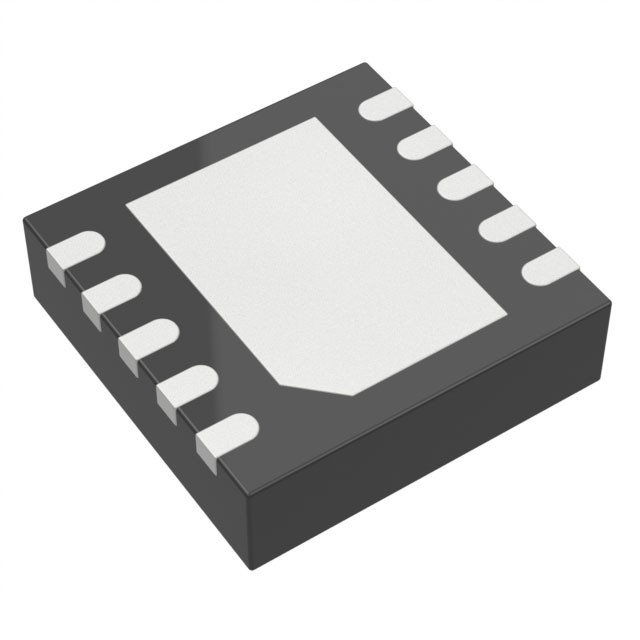
LTC4413EDD-2#PBF
ActiveDUAL 2.6A, 2.5V TO 5.5V FAST IDEAL DIODES IN A 3MM × 3MM DFN
Deep-Dive with AI
Search across all available documentation for this part.

LTC4413EDD-2#PBF
ActiveDUAL 2.6A, 2.5V TO 5.5V FAST IDEAL DIODES IN A 3MM × 3MM DFN
Deep-Dive with AI
Technical Specifications
Parameters and characteristics for this part
| Specification | LTC4413EDD-2#PBF |
|---|---|
| Applications | Handheld/Mobile Devices |
| Current - Output (Max) [Max] | 2.6 A |
| Current - Supply | 40 µA |
| Delay Time - OFF | 2 µs |
| Delay Time - ON | 11 µs |
| FET Type | P-Channel |
| Internal Switch(s) | True |
| Mounting Type | Surface Mount |
| Operating Temperature [Max] | 85 °C |
| Operating Temperature [Min] | -40 °C |
| Package / Case | 10-WFDFN Exposed Pad |
| Ratio - Input:Output | 2:1 |
| Supplier Device Package | 10-DFN (3x3) |
| Type | Source Selector Switch |
| Voltage - Supply [Max] | 5.5 V |
| Voltage - Supply [Min] | 2.5 V |
Pricing
Prices provided here are for design reference only. For realtime values and availability, please visit the distributors directly
| Distributor | Package | Quantity | $ | |
|---|---|---|---|---|
| Digikey | Tube | 1 | $ 8.47 | |
| 10 | $ 5.83 | |||
| 25 | $ 5.14 | |||
| 100 | $ 4.38 | |||
| 250 | $ 4.01 | |||
| 500 | $ 3.78 | |||
| 1000 | $ 3.59 | |||
| 2500 | $ 3.46 | |||
Description
General part information
LTC4413-1LTC4413-2 Series
The LTC4413-1 and LTC4413-2 each contain two monolithic ideal diodes, each capable of supplying up to 2.6A from input voltages between 2.5V and 5.5V. The ideal diodes use a 100mΩ P-channel MOSFET to independently connect INA to OUTA and INB to OUTB. During normal forward operation, the voltage drops across each of these diodes are regulated to as low as 18mV. Quiescent current is less than 80µA for diode currents up to 1A. If either of the output voltages exceeds its respective input voltage, that MOSFET is turned off and less than 1µA of reverse current flows from OUT to IN. Maximum forward current in each MOSFET is limited to a constant 2.6A and internal thermal limiting circuits protect the part during fault conditions. An internal overvoltage protection sensor detects when a voltage exceeds the LTC4413-2 absolute maximum voltage tolerance.Two active-high control pins independently turn off the two ideal diodes contained within the LTC4413-1/LTC4413-2. When the selected channel is reverse biased, or the LTC4413-1/LTC4413-2 is put into low power standby, the status signal is pulled low by an 11µA open drain.The LTC4413-1/LTC4413-2 are housed in a 10-lead 3mm × 3mm DFN package.FeaturesLTC4413Lower IqLTC4413-1Lower Vfwd, Faster Response, Higher IqLTC4413-2Lower Vfwd, Faster Response, Higher Iq, 13V (max) OVPApplicationsBattery and Wall Adapter Diode OR’ing in Handheld ProductsBackup Battery Diode OR’ingPower SwitchingUSB PeripheralsUninterruptable Supplies
Documents
Technical documentation and resources


