AD673SD
Active8-BIT SUCCESSIVE APPROXIMATION, ADC
Deep-Dive with AI
Search across all available documentation for this part.
AD673SD
Active8-BIT SUCCESSIVE APPROXIMATION, ADC
Deep-Dive with AI
Technical Specifications
Parameters and characteristics for this part
| Specification | AD673SD |
|---|---|
| Architecture | SAR |
| Configuration | S/H-ADC |
| Data Interface | Parallel |
| Input Type | Single Ended |
| Mounting Type | Through Hole |
| Number of A/D Converters | 1 |
| Number of Bits | 8 |
| Number of Inputs | 1 |
| Operating Temperature [Max] | 125 °C |
| Operating Temperature [Min] | -55 °C |
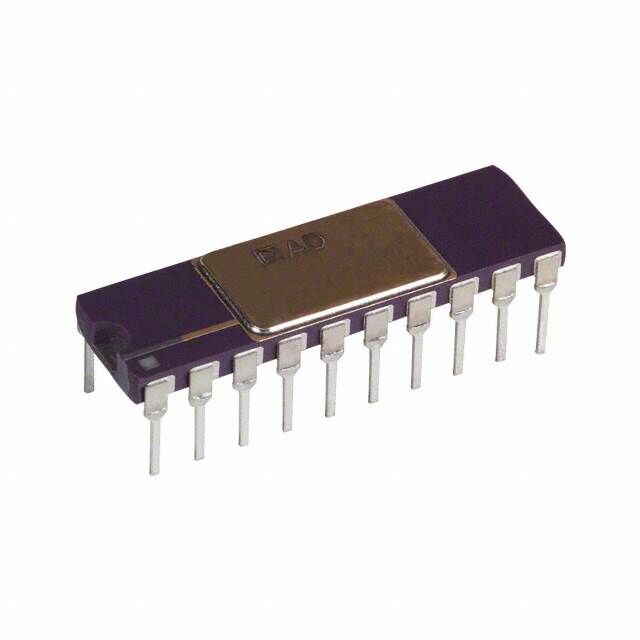
| Package / Case | 20-CDIP |
| Ratio - S/H:ADC | 1:1 |
| Reference Type | Internal |
| Supplier Device Package | 20-CDIP |
| Voltage - Supply, Analog [Max] | 16.5 V, 7 V |
| Voltage - Supply, Analog [Min] | 4.5 V, -12 V |
| Voltage - Supply, Digital [Max] | 7 V, 16.5 V |
| Voltage - Supply, Digital [Min] | 4.5 V, -12 V |
Pricing
Prices provided here are for design reference only. For realtime values and availability, please visit the distributors directly
| Distributor | Package | Quantity | $ | |
|---|---|---|---|---|
| Digikey | Tube | 2 | $ 243.99 | |
| 10 | $ 222.94 | |||
Description
General part information
5962-8850502 Series
The AD673 is a complete 8-bit successive approximation analog-to-digital converter consisting of a DAC, voltage reference, clock, comparator, successive approximation register (SAR) and 3-state output buffers-all fabricated on a single chip. No external components are required to perform a full ac-curacy 8-bit conversion in 20 µs.The AD673 incorporates advanced integrated circuit design and processing technologies. The successive approximation function is implemented with I2L (integrated injection logic). Laser trimming of the high stability SiCr thin-film resistor ladder network insures high accuracy, which is maintained with a temperature compensated sub-surface Zener reference.Operating on supplies of +5 V and −12 V to −15 V, the AD673 will accept analog inputs of 0 V to +10 V or −5 V to +5 V. The trailing edge of a positive pulse on the CONVERT line initiates the 20 µs conversion cycle.DATA READYindicates completion of the conversion.The AD673 is available in two versions. The AD673J as specified over the 0°C to +70°C temperature range and the AD673S guarantees ±1/2 LSB relative accuracy and no missing codes from −55°C to +125°C.Two package configurations are offered. All versions are also offered in a 20-pin hermetically sealed ceramic DIP. The AD673J is also available in a 20-pin plastic DIP.
Documents
Technical documentation and resources