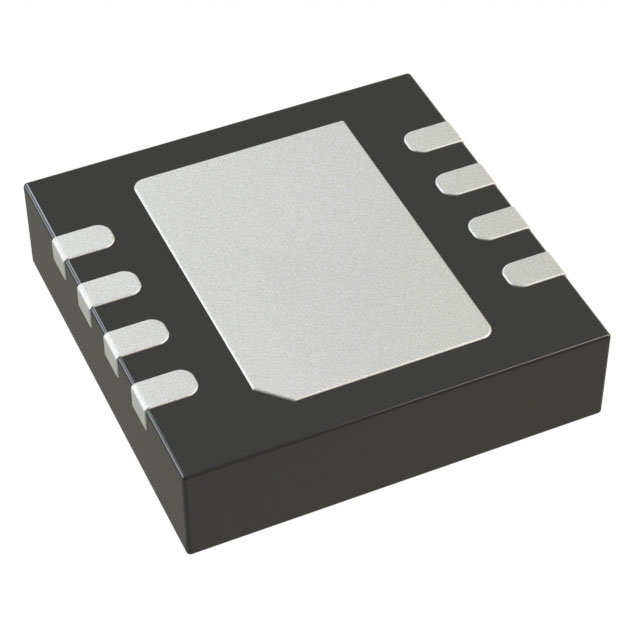
SSM2301CPZ-REEL7
ObsoleteFILTERLESS HIGH EFFICIENCY MONO 1.4 W CLASS-D AUDIO AMPLIFIER
Deep-Dive with AI
Search across all available documentation for this part.

SSM2301CPZ-REEL7
ObsoleteFILTERLESS HIGH EFFICIENCY MONO 1.4 W CLASS-D AUDIO AMPLIFIER
Technical Specifications
Parameters and characteristics for this part
| Specification | SSM2301CPZ-REEL7 |
|---|---|
| Features | Short-Circuit and Thermal Protection, Differential Inputs, Depop, Shutdown |
| Max Output Power x Channels @ Load | 1.52 W |
| Max Output Power x Channels @ Load [custom] | 8 Ohm |
| Max Output Power x Channels @ Load [x] | 1 |
| Mounting Type | Surface Mount |
| Operating Temperature [Max] | 85 °C |
| Operating Temperature [Min] | -40 °C |
| Output Type | 1-Channel (Mono) |
| Package / Case | 8-VFDFN Exposed Pad, CSP |
| Supplier Device Package | 8-LFCSP-VD (3x3) |
| Type | Class D |
| Voltage - Supply [Max] | 5 V |
| Voltage - Supply [Min] | 2.5 V |
Pricing
Prices provided here are for design reference only. For realtime values and availability, please visit the distributors directly
| Distributor | Package | Quantity | $ | |
|---|---|---|---|---|
Description
General part information
SSM2301 Series
The SSM2301 is a fully integrated, high efficiency, Class-D audio amplifier designed to maximize performance for mobile phone applications. The application circuit requires a minimum of external components and operates from a single 2.5 V to 5.0 V supply. It is capable of delivering 1.4 W of continuous output power with less than 1% THD + N driving an 8 Ω load from a 5.0 V supply.The SSM2301 features a high efficiency, low noise modulation scheme that does not require external LC output filters. The modulation provides high efficiency even at low output power. The SSM2301 operates with 85% efficiency at 1.4 W into 8 Ω from a 5.0 V supply and has a signal-to-noise ratio (SNR) that is greater than 98 dB. Spread-spectrum modulation is used to provide lower EMI-radiated emissions compared with other Class-D architectures.The SSM2301 has a micropower shutdown mode with a maximum shutdown current of 30 nA. Shutdown is enabled by applying a logic low to theSDpin.The device also includes pop-and-click suppression circuitry. This minimizes voltage glitches at the output during turn-on and turn-off, thus reducing audible noise on activation and deactivation.The fully differential input of the SSM2301 provides excellent rejection of common-mode noise on the input. Input coupling capacitors can be omitted if the dc input common-mode voltage is approximately VDD/2.The SSM2301 also has excellent rejection of power supply noise, including noise caused by GSM transmission bursts and RF rectification. PSRR is typically 63 dB at 217 Hz.The gain can be set to 6 dB or 12 dB by utilizing the gain control select pin connected respectively to ground or to VDD. Gain can also be adjusted externally by inserting a resistor in series with each input pin.The SSM2301 is specified over the commercial temperature range (−40°C to +85°C). It has built-in thermal shutdown and output short-circuit protection. It is available in both an 8-lead, 3 mm × 3 mm lead-frame chip scale package (LFCSP) and an 8-lead MSOP package.ApplicationsMobile phonesMP3 playersPortable gamingPortable electronicsEducational toys
Documents
Technical documentation and resources


