LTC6416CDDB#TRPBF
LTB2GHZ LOW NOISE DIFFERENTIAL 16-BIT ADC BUFFER
Deep-Dive with AI
Search across all available documentation for this part.
LTC6416CDDB#TRPBF
LTB2GHZ LOW NOISE DIFFERENTIAL 16-BIT ADC BUFFER
Deep-Dive with AI
Technical Specifications
Parameters and characteristics for this part
| Specification | LTC6416CDDB#TRPBF |
|---|---|
| -3db Bandwidth | 2 GHz |
| Amplifier Type | Buffer |
| Current - Input Bias | 5 µA |
| Current - Output / Channel | 20 mA |
| Current - Supply | 42 mA |
| Mounting Type | Surface Mount |
| Number of Circuits | 1 |
| Operating Temperature [Max] | 70 °C |
| Operating Temperature [Min] | 0 °C |
| Output Type | Differential |
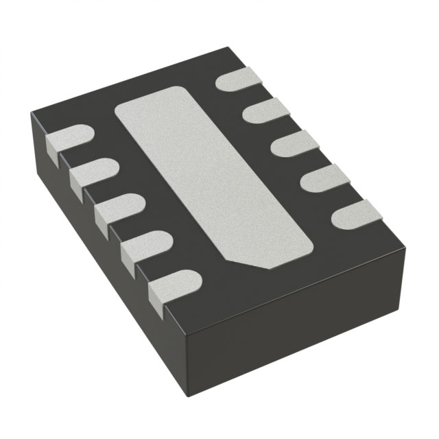
| Package / Case | 10-WFDFN Exposed Pad |
| Slew Rate | 3400 V/µs |
| Supplier Device Package | 10-DFN (3x2) |
| Voltage - Input Offset | 500 çV |
| Voltage - Supply Span (Max) [Max] | 3.9 V |
| Voltage - Supply Span (Min) [Min] | 2.7 V |
Pricing
Prices provided here are for design reference only. For realtime values and availability, please visit the distributors directly
| Distributor | Package | Quantity | $ | |
|---|---|---|---|---|
| Digikey | Tape & Reel (TR) | 2500 | $ 5.22 | |
Description
General part information
LTC6416 Series
The LTC6416 is a differential unity gain buffer designed to drive 16-bit ADCs with extremely low output noise and excellent linearity beyond 300MHz. Differential input impedance is 12kΩ, allowing 1:4 and 1:8 transformers to be used at the input to achieve additional system gain.With no external biasing or gain setting components and a flow-through pinout, the LTC6416 is very easy to use. It can be DC-coupled and has a common mode output offset of –40mV. If the input signals are AC-coupled, the LTC6416 input pins are internally biased to provide an output common mode voltage that is set by the voltage on the VCMpin.In addition the LTC6416 has high speed, fast recovery clamping circuitry to limit output signal swing. Both the high and low clamp voltages are internally biased to allow maximum output swing but are also user programmable via the CLLO and CLHI pins.Supply current is nominally 42mA and the LTC6416 operates on supply voltages ranging from 2.7V to 3.9V.The LTC6416 is packaged in a 10-lead 3mm × 2mm DFN package. Pinout is optimized for placement directly adjacent to Linear’s high speed 12-, 14- and 16-bit ADCs.ApplicationsDifferential ADC DriverIF Sampling ReceiversImpedance TransformerSAW Filter InterfaceCCD Buffer
Documents
Technical documentation and resources