5962-0051401VPA
ActiveRADIATION-TOLERANT QMLV, 3-A/3-A DUAL-CHANNEL GATE DRIVER WITH 35-V VDD
Deep-Dive with AI
Search across all available documentation for this part.
5962-0051401VPA
ActiveRADIATION-TOLERANT QMLV, 3-A/3-A DUAL-CHANNEL GATE DRIVER WITH 35-V VDD
Technical Specifications
Parameters and characteristics for this part
| Specification | 5962-0051401VPA |
|---|---|
| Channel Type | Independent |
| Current - Peak Output (Source, Sink) [custom] | 3 A |
| Current - Peak Output (Source, Sink) [custom] | 3 A |
| Driven Configuration | Low-Side |
| Gate Type | N-Channel, P-Channel MOSFET |
| Grade | Military |
| Input Type | Non-Inverting |
| Logic Voltage - VIL, VIH | 0.8 V, 2 V |
| Mounting Type | Through Hole |
| Number of Drivers | 2 |
| Operating Temperature [Max] | 125 °C |
| Operating Temperature [Min] | -55 °C |
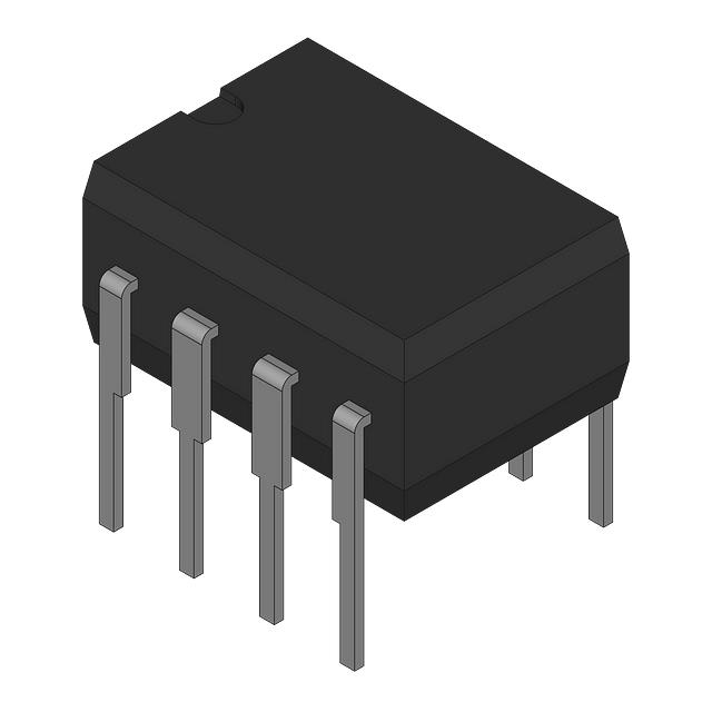
| Package / Case | 7.62 mm |
| Package / Case | 0.3 in |
| Package / Case | 8-CDIP |
| Qualification | MIL-PRF-38535L |
| Rise / Fall Time (Typ) [custom] | 25 ns |
| Rise / Fall Time (Typ) [custom] | 25 ns |
| Supplier Device Package | 8-CDIP |
| Voltage - Supply [Max] | 35 V |
| Voltage - Supply [Min] | 5 V |
Pricing
Prices provided here are for design reference only. For realtime values and availability, please visit the distributors directly
| Distributor | Package | Quantity | $ | |
|---|---|---|---|---|
| Digikey | Bulk | 2 | $ 209.96 | |
| Texas Instruments | TUBE | 1 | $ 200.59 | |
| 10 | $ 183.88 | |||
| 100 | $ 167.16 | |||
Description
General part information
5962-0051401 Series
The UC1708 family of power drivers is made with a high-speed, high-voltage, Schottky process to interface control functions and high-power switching devices — particularly power MOSFETs. Operating over a 5 V to 35 V supply range, these devices contain two independent channels. The A and B inputs are compatible with TTL and CMOS logic families, but can withstand input voltages as high as VIN. Each output can source or sink up to 3 A as long as power dissipation limits are not exceeded.
Although each output can be activated independently with its own inputs, they can be forced low in common through the action of either a digital high signal at the Shutdown terminal or by forcing the Enable terminal low. The Shutdown terminal will only force the outputs low, it will not effect the behavior of the rest of the device. The Enable terminal effectively places the device in under-voltage lockout, reducing power consumption by as much as 90%. During under-voltage and disable (Enable terminal forced low) conditions, the outputs are held in a self-biasing, low-voltage, state.
The UC3708 and UC2708 are available in plastic 8-pin MINI DIP and 16-pinbat-wingDIP packages for commercial operation over a 0°C to 70°C temperature range and industrial temperature range of -25°C to 85°C respectively. For operation over a -55°C to 125°C temperature range, the UC1708 is available in hermetically sealed 8-pin MINI CDIP, 16 pin CDIP and 20 pin CLCC packages. Surface mount devices are also available.
Documents
Technical documentation and resources