5V49EE701NDGI8
ObsoleteEEPROM PROGRAMMABLE CLOCK GENERATOR
Deep-Dive with AI
Search across all available documentation for this part.
5V49EE701NDGI8
ObsoleteEEPROM PROGRAMMABLE CLOCK GENERATOR
Deep-Dive with AI
Technical Specifications
Parameters and characteristics for this part
| Specification | 5V49EE701NDGI8 |
|---|---|
| Differential - Input:Output | No/Yes |
| Frequency - Max [Max] | 500 MHz |
| Input | LVTTL, Crystal, LVCMOS |
| Mounting Type | Surface Mount |
| Number of Circuits | 1 |
| Operating Temperature [Max] | 85 °C |
| Operating Temperature [Min] | -40 °C |
| Output | LVTTL, LVCMOS, LVDS, HCSL, LVPECL |
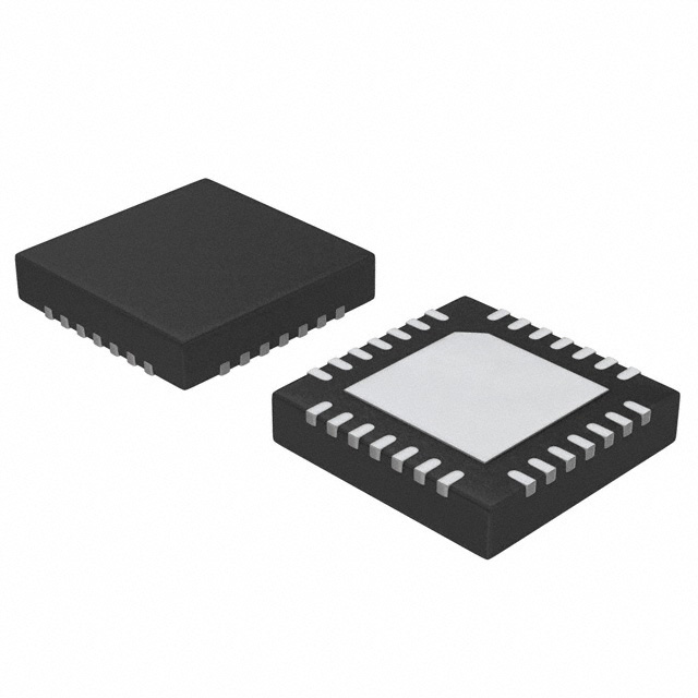
| Package / Case | 28-VQFN Exposed Pad |
| PLL | Yes with Bypass |
| Ratio - Input:Output [custom] | 6 |
| Ratio - Input:Output [custom] | 2 |
| Supplier Device Package | 28-VFQFPN (6x6) |
| Type | Clock Generator, Multiplexer |
| Voltage - Supply [Max] | 3.465 V |
| Voltage - Supply [Min] | 3.135 V |
Pricing
Prices provided here are for design reference only. For realtime values and availability, please visit the distributors directly
| Distributor | Package | Quantity | $ | |
|---|---|---|---|---|
Description
General part information
5V49EE701 Series
The 5V49EE701 is a programmable clock generator intended for high performance data-communications, telecommunications, consumer, and networking applications. There are four internal PLLs, each individually programmable, allowing for four unique non-integer-related frequencies. The frequencies are generated from a single reference clock. The reference clock can come from one of the two redundant clock inputs. Automatic or manual switchover function allows any one of the redundant clocks to be selected during normal operation. The 5V49EE701 is in-system, programmable and can be programmed through the use of I2C interface. An internal EEPROM allows the user to save and restore the configuration of the device without having to reprogram it on power-up. Each of the four PLLs has an 7-bit reference divider and a 12-bit feedback divider. This allows the user to generate four unique non-integer-related frequencies. The PLL loop bandwidth is programmable to allow the user to tailor the PLL response to the application. For instance, the user can tune the PLL parameters to minimize jitter generation or to maximize jitter attenuation. Spread spectrum generation and/or fractional divides are allowed on two of the PLLs. There are a total of five 8-bit output dividers. Each output bank can be configured to support LVTTL, LVPECL, LVDS or HCSL logic levels. Out0 (Output 0) supports 3.3V single-ended output only. The outputs are connected to the PLLs via a switch matrix. The switch matrix allows the user to route the PLL outputs to any output bank. This feature can be used to simplify and optimize the board layout. In addition, each output's slew rate and enable/disable function is programmable.
Documents
Technical documentation and resources
No documents available