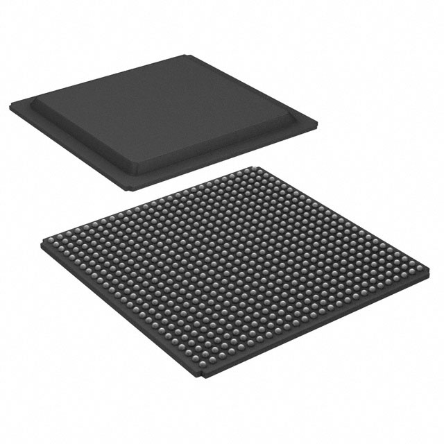
XCKU5P-1FFVB676E
ActiveFPGA, KINTEX ULTRASCALE+, MMCM, PLL, 280 I/O'S, 630 MHZ, 474600 CELLS, 825 -876 MV, FCBGA-676, NCNR
Deep-Dive with AI
Search across all available documentation for this part.

XCKU5P-1FFVB676E
ActiveFPGA, KINTEX ULTRASCALE+, MMCM, PLL, 280 I/O'S, 630 MHZ, 474600 CELLS, 825 -876 MV, FCBGA-676, NCNR
Deep-Dive with AI
Technical Specifications
Parameters and characteristics for this part
| Specification | XCKU5P-1FFVB676E |
|---|---|
| Mounting Type | Surface Mount |
| Number of I/O | 280 |
| Number of LABs/CLBs | 27120 |
| Number of Logic Elements/Cells | 474600 |
| Operating Temperature [Max] | 100 °C |
| Operating Temperature [Min] | 0 °C |
| Supplier Device Package | 676-FCBGA (27x27) |
| Total RAM Bits | 41984000 Bits |
| Voltage - Supply [Max] | 0.876 V |
| Voltage - Supply [Min] | 0.825 V |
Pricing
Prices provided here are for design reference only. For realtime values and availability, please visit the distributors directly
Description
General part information
XCKU5 Series
The Xilinx Kintex® UltraScale+™ FPGA family provide the best price/performance/watt balance in a FinFET node delivering the most cost effective solution for high end capabilities including transceiver and memory interface line rates as well as 100G connectivity cores. The Kintex® UltraScale+™ FPGAs are available in -3, -2, -1 speed grades. This newest mid-range family is ideal for both packet processing and DSP intensive functions and is well suited for applications ranging from wireless MIMO technology to Nx100G networking and data centre. Based on the UltraScale™ architecture, these devices have increased performance and on-chip UltraRAM memory to reduce BOM cost providing the ideal mix of high performance peripherals and cost effective system implementation. In addition, Kintex® UltraScale+™ FPGAs have numerous power options that deliver the optimal balance between the required system performance and the smallest power envelope.
Documents
Technical documentation and resources


