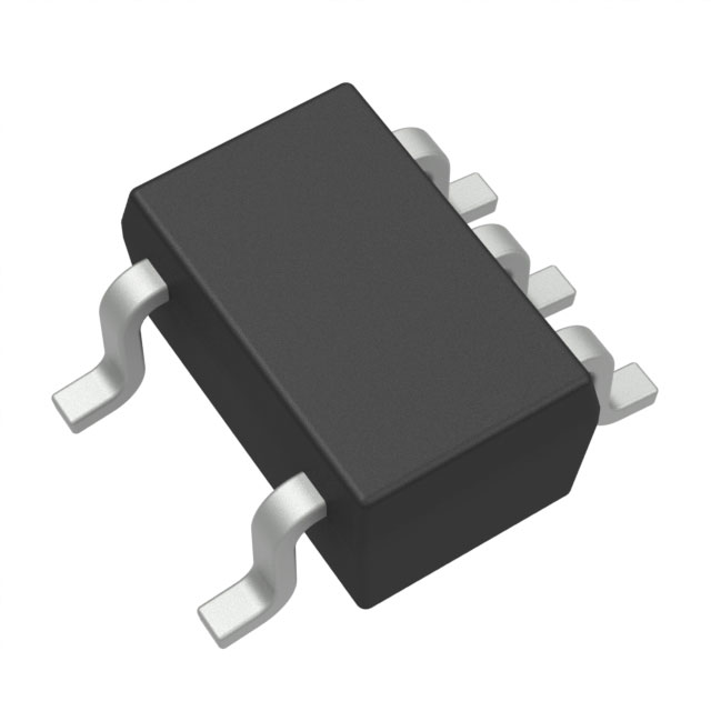
2N7001TDCKR
Active1-BIT DUAL-SUPPLY BUFFERED VOLTAGE SIGNAL CONVERTER
Deep-Dive with AI
Search across all available documentation for this part.

2N7001TDCKR
Active1-BIT DUAL-SUPPLY BUFFERED VOLTAGE SIGNAL CONVERTER
Deep-Dive with AI
Technical Specifications
Parameters and characteristics for this part
| Specification | 2N7001TDCKR |
|---|---|
| Channel Type | Unidirectional |
| Channels per Circuit | 1 |
| Data Rate | 100 Mbps |
| Input Signal | CMOS |
| Mounting Type | Surface Mount |
| Number of Circuits | 1 |
| Operating Temperature [Max] | 125 °C |
| Operating Temperature [Min] | -40 °C |
| Output Signal | CMOS |
| Output Type | Push-Pull |
| Package / Case | SC-70-5, 5-TSSOP, SOT-353 |
| Supplier Device Package | SC-70-5 |
| Translator Type | Voltage Level |
| Voltage - VCCA [Max] | 3.6 V |
| Voltage - VCCA [Min] | 1.65 V |
| Voltage - VCCB [Max] | 3.6 V |
| Voltage - VCCB [Min] | 1.65 V |
Pricing
Prices provided here are for design reference only. For realtime values and availability, please visit the distributors directly
| Distributor | Package | Quantity | $ | |
|---|---|---|---|---|
| Digikey | Cut Tape (CT) | 1 | $ 0.53 | |
| 10 | $ 0.45 | |||
| 100 | $ 0.32 | |||
| 500 | $ 0.25 | |||
| 1000 | $ 0.20 | |||
| Digi-Reel® | 1 | $ 0.53 | ||
| 10 | $ 0.45 | |||
| 100 | $ 0.32 | |||
| 500 | $ 0.25 | |||
| 1000 | $ 0.20 | |||
| Tape & Reel (TR) | 3000 | $ 0.18 | ||
| 6000 | $ 0.17 | |||
| 9000 | $ 0.16 | |||
| 30000 | $ 0.15 | |||
| Texas Instruments | LARGE T&R | 1 | $ 0.23 | |
| 100 | $ 0.16 | |||
| 250 | $ 0.12 | |||
| 1000 | $ 0.08 | |||
Description
General part information
2N7001T-Q1 Series
The AEC-Q100 qualified 2N7001T-Q1 device is a single-bit buffered voltage signal converter that uses two separate configurable power-supply rails to up or down translate a unidirectional signal. The device is operational with both VCCAand VCCBsupplies down to 1.65 V and up to 3.60 V. VCCAdefines the input threshold voltage on the A input. VCCBdefines the output drive voltage on the B output.
This device is fully specified for partial-power-down applications using the Ioffcurrent. The Ioffprotection circuitry ensures that no excessive current is drawn from or to an input, output, or combined I/O that is biased to a specific voltage while the device is powered down.
The VCCisolation feature ensures that if either VCCAor VCCBis less than 100 mV, the output port (B) enters a high-impedance state.
Documents
Technical documentation and resources


