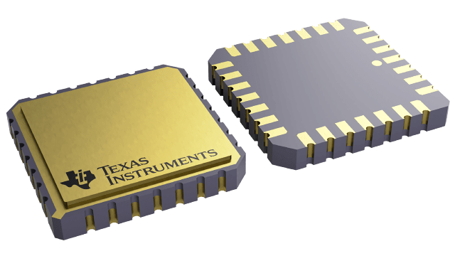
SNJ54ALS653FK
ActiveOCTAL BUS TRANSCEIVERS AND REGISTERS WITH 3-STATE OUTPUTS
Deep-Dive with AI
Search across all available documentation for this part.

SNJ54ALS653FK
ActiveOCTAL BUS TRANSCEIVERS AND REGISTERS WITH 3-STATE OUTPUTS
Technical Specifications
Parameters and characteristics for this part
| Specification | SNJ54ALS653FK |
|---|---|
| Current - Output High, Low [custom] | 12 mA |
| Current - Output High, Low [custom] | 12 mA |
| Logic Type | Transceiver, Inverting |
| Mounting Type | Surface Mount |
| Number of Bits per Element | 8 |
| Number of Elements | 1 |
| Operating Temperature [Max] | 125 °C |
| Operating Temperature [Min] | -55 °C |
| Output Type | 3-State, Open Collector |
| Package / Case | 28-CLCC |
| Supplier Device Package | 28-LCCC |
| Supplier Device Package [x] | 11.43 |
| Supplier Device Package [y] | 11.43 |
| Voltage - Supply [Max] | 5.5 V |
| Voltage - Supply [Min] | 4.5 V |
Pricing
Prices provided here are for design reference only. For realtime values and availability, please visit the distributors directly
| Distributor | Package | Quantity | $ | |
|---|---|---|---|---|
| Texas Instruments | TUBE | 1 | $ 70.00 | |
| 100 | $ 62.22 | |||
| 250 | $ 51.15 | |||
| 1000 | $ 45.75 | |||
Description
General part information
5962-89687013 Series
These devices consist of bus-transceiver circuits, D-type flip-flops, and control circuitry arranged for multiplexed transmission of data directly from the data bus or from the internal storage registers. Output-enable (OEAB and OEBA\) inputs are provided to control the transceiver functions. Select-control (SAB and SBA) inputs are provided to select real-time or stored data transfer. The circuitry used for select control eliminates the typical decoding glitch that occurs in a multiplexer during the transition between stored and real-time data. A low input level selects real-time data, and a high input level selects stored data. Figure 1 illustrates the four fundamental bus-management functions that can be performed with the octal bus transceivers and registers
Data on the A or B data bus, or both, can be stored in the internal D-type flip-flops by low-to-high transitions at the appropriate clock (CLKAB or CLKBA) terminals, regardless of the select- or output-control terminals. When SAB and SBA are in the real-time transfer mode, it is possible to store data without using the internal D-type flip-flops by simultaneously enabling OEAB and OEBA\. In this configuration, each output reinforces its input. When all other data sources to the two sets of bus lines are at high impedance, each set of bus lines remains at its last state.
The -1 versions of the SN74ALS651A and SN74ALS652A are identical to the standard versions except that the recommended maximum IOLfor the -1 versions is increased to 48 mA. There are no -1 versions of the SN54ALS652, SN54ALS653, SN74ALS653, and SN74ALS654.
Documents
Technical documentation and resources


