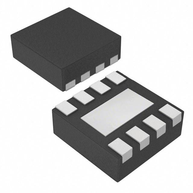
UCC27523DSDT
ActiveIC GATE DRVR LOW-SIDE 8SON
Deep-Dive with AI
Search across all available documentation for this part.

UCC27523DSDT
ActiveIC GATE DRVR LOW-SIDE 8SON
Deep-Dive with AI
Technical Specifications
Parameters and characteristics for this part
| Specification | UCC27523DSDT |
|---|---|
| Channel Type | Independent |
| Current - Peak Output (Source, Sink) [custom] | 5 A |
| Current - Peak Output (Source, Sink) [custom] | 5 A |
| Driven Configuration | Low-Side |
| Gate Type | N-Channel MOSFET, IGBT |
| Input Type | Inverting |
| Logic Voltage - VIL, VIH | 1 V, 2.3 V |
| Mounting Type | Surface Mount |
| Number of Drivers | 2 |
| Operating Temperature [Max] | 140 °C |
| Operating Temperature [Min] | -40 °C |
| Package / Case | 8-WDFN Exposed Pad |
| Rise / Fall Time (Typ) [custom] | 7 ns |
| Rise / Fall Time (Typ) [custom] | 6 ns |
| Supplier Device Package | 8-SON (3x3) |
| Voltage - Supply [Max] | 18 V |
| Voltage - Supply [Min] | 4.5 V |
Pricing
Prices provided here are for design reference only. For realtime values and availability, please visit the distributors directly
| Distributor | Package | Quantity | $ | |
|---|---|---|---|---|
| Digikey | Cut Tape (CT) | 1 | $ 2.55 | |
| 10 | $ 2.29 | |||
| 25 | $ 2.16 | |||
| 100 | $ 1.84 | |||
| Digi-Reel® | 1 | $ 2.55 | ||
| 10 | $ 2.29 | |||
| 25 | $ 2.16 | |||
| 100 | $ 1.84 | |||
| Tape & Reel (TR) | 250 | $ 1.73 | ||
| 500 | $ 1.51 | |||
| 1250 | $ 1.25 | |||
| 2500 | $ 1.17 | |||
| 6250 | $ 1.12 | |||
Description
General part information
UCC27523 Series
The UCC2752x family of devices are dual-channel, high-speed, low-side gate-driver devices capable of effectively driving MOSFET and IGBT power switches. Using a design that inherently minimizes shoot-through current, UCC2752x can deliver high-peak current pulses of up to 5A source and 5A sink into capacitive loads along with rail-to-rail drive capability and extremely small propagation delay (typically 13ns). In addition, the drivers feature matched internal propagation delays between the two channels. These delays are very well suited for applications requiring dual-gate drives with critical timing, such as synchronous rectifiers. This also enables connecting two channels in parallel to effectively increase current-drive capability or driving two switches in parallel with one input signal. The input pin thresholds are based on TTL and CMOS compatible low-voltage logic, which is fixed and independent of the VDD supply voltage. Wide hysteresis between the high and low thresholds offers excellent noise immunity.
The UCC2752x family provides the combination of three standard logic options — dual inverting, dual noninverting, one inverting and one noninverting driver. The UCC27526 features a dual input design which offers flexibility of both inverting (IN– pin) and non-inverting (IN+ pin) configuration for each channel. Either IN+ or IN– pin controls the state of the driver output. The unused input pin is used for enable and disable functions. For safety purpose, internal pullup and pulldown resistors on the input pins of all the devices in UCC2752x family ensure that outputs are held LOW when input pins are in floating condition. The UCC27523 and UCC27525 devices feature Enable pins (ENA and ENB) to have better control of the operation of the driver applications. The pins are internally pulled up to VDD for active-high logic and are left open for standard operation.
The UCC2752x family of devices are available in SOIC-8 (D), MSOP-8 with exposed pad (DGN) and 3mm × 3mm WSON-8 with exposed pad (DSD) packages. The UCC27526 is only offered in a 3mm × 3mm WSON (DSD) package.
Documents
Technical documentation and resources
No documents available


