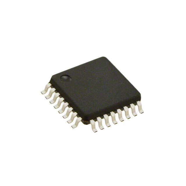
5V9885TPFGI
Obsolete3.3V EEPROM PROGRAMMABLE CLOCK GENERATOR
Deep-Dive with AI
Search across all available documentation for this part.

5V9885TPFGI
Obsolete3.3V EEPROM PROGRAMMABLE CLOCK GENERATOR
Deep-Dive with AI
Technical Specifications
Parameters and characteristics for this part
| Specification | 5V9885TPFGI |
|---|---|
| Differential - Input:Output | No/Yes |
| Frequency - Max [Max] | 500 MHz |
| Input | LVCMOS, LVTTL |
| Mounting Type | Surface Mount |
| Number of Circuits | 1 |
| Operating Temperature [Max] | 85 °C |
| Operating Temperature [Min] | -40 °C |
| Output | LVTTL, LVDS, LVCMOS, LVPECL |
| Package / Case | 32-LQFP |
| PLL | Yes with Bypass |
| Ratio - Input:Output [custom] | 6 |
| Ratio - Input:Output [custom] | 2 |
| Supplier Device Package | 32-TQFP (7x7) |
| Voltage - Supply [Max] | 3.6 V |
| Voltage - Supply [Min] | 3 V |
Pricing
Prices provided here are for design reference only. For realtime values and availability, please visit the distributors directly
| Distributor | Package | Quantity | $ | |
|---|---|---|---|---|
Description
General part information
5V9885T Series
The IDT5V9885T is a programmable clock generator intended for high performance data-communications, telecommunications, consumer, andnetworking applications. There are three internal PLLs, each individually programmable, allowing for three unique non-integer-related frequencies. The frequencies are generated from a single reference clock. The reference clock can come from one of the two redundant clock inputs. A glitchless automatic or manual switchover function allows any one of theredundant clocks to be selected during normal operation.The IDT5V9885T can be programmed through the use of the I2C or JTAG interfaces. The programming interface enables the device to be programmed when it is in normal operation or what is commonly known as in-system programmable. An internal EEPROM allows the user to save and restore the configuration of the device without having to reprogram it on power-up. JTAG boundary scan is also implemented.Each of the three PLLs has an 8-bit pre-scaler and a 12-bit feedback divider. This allows the user to generate three unique non-integer-related frequencies. The PLL loop bandwidth is programmable to allow the user to tailor the PLL response to the application. For instance, the user can tune the PLL parameters to minimize jitter generation or to maximize jitter attenuation. Spread spectrum generation and fractional divides are allowed on two of the PLLs.There are 10-bit post dividers on five of the six output banks. Two of the six output banks are configurable to be LVTTL, LVPECL, or LVDS. Theother four output banks are LVTTL. The outputs are connected to the PLLs via the switch matrix. The switch matrix allows the user to route the PLL outputs to any output bank. This feature can be used to simplify and optimize the board layout. In addition, each output's slew rate and enable/disablefunction can be programmed.
Documents
Technical documentation and resources


