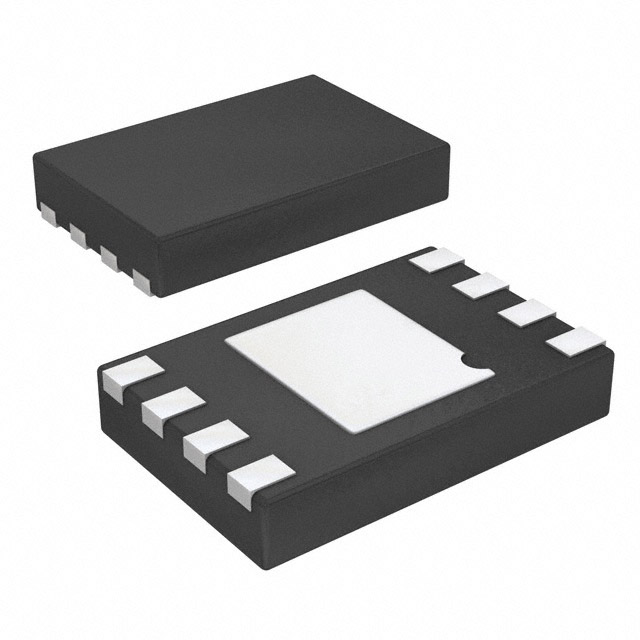
BD00GA3WNUX-TR
ActiveLDO, ADJ, 1.5-13V, 0.3A, -25 TO 85DEG C ROHS COMPLIANT: YES
Deep-Dive with AI
Search across all available documentation for this part.

BD00GA3WNUX-TR
ActiveLDO, ADJ, 1.5-13V, 0.3A, -25 TO 85DEG C ROHS COMPLIANT: YES
Deep-Dive with AI
Technical Specifications
Parameters and characteristics for this part
| Specification | BD00GA3WNUX-TR |
|---|---|
| Control Features | Soft Start, Enable |
| Current - Output | 300 mA |
| Current - Quiescent (Iq) | 0.6 mA |
| Current - Supply (Max) [Max] | 900 µA |
| Mounting Type | Surface Mount |
| Number of Regulators | 1 |
| Operating Temperature [Max] | 85 °C |
| Operating Temperature [Min] | -25 °C |
| Output Configuration | Positive |
| Output Type | Adjustable |
| Package / Case | 8-UFDFN Exposed Pad |
| Protection Features | Soft Start, Over Temperature, Over Current |
| Supplier Device Package | VSON008X2030 |
| Voltage - Input (Max) [Max] | 14 V |
| Voltage - Output (Max) [Max] | 13 V |
| Voltage - Output (Min/Fixed) | 1.5 V |
| Voltage Dropout (Max) [Max] | 0.9 V |
Pricing
Prices provided here are for design reference only. For realtime values and availability, please visit the distributors directly
| Distributor | Package | Quantity | $ | |
|---|---|---|---|---|
| Digikey | Cut Tape (CT) | 1 | $ 1.14 | |
| 10 | $ 0.71 | |||
| 25 | $ 0.60 | |||
| 100 | $ 0.47 | |||
| 250 | $ 0.41 | |||
| 500 | $ 0.37 | |||
| 1000 | $ 0.34 | |||
| Digi-Reel® | 1 | $ 1.14 | ||
| 10 | $ 0.71 | |||
| 25 | $ 0.60 | |||
| 100 | $ 0.47 | |||
| 250 | $ 0.41 | |||
| 500 | $ 0.37 | |||
| 1000 | $ 0.34 | |||
| Tape & Reel (TR) | 4000 | $ 0.29 | ||
| 8000 | $ 0.27 | |||
| 12000 | $ 0.26 | |||
| 20000 | $ 0.25 | |||
| 28000 | $ 0.24 | |||
| 40000 | $ 0.24 | |||
| Newark | Each (Supplied on Cut Tape) | 1 | $ 0.72 | |
| 10 | $ 0.61 | |||
| 25 | $ 0.54 | |||
| 50 | $ 0.48 | |||
| 100 | $ 0.41 | |||
| 250 | $ 0.39 | |||
| 500 | $ 0.37 | |||
| 1000 | $ 0.33 | |||
Description
General part information
BD00GA3WNUX Series
BDxxGA3WEFJ / BDxxGA3WNUX series devices are LDO regulators with output current capability of 0.3A. It has an output voltage accuracy of ±1%. Both fixed and variable output voltage devices are available. The variable output voltage can be varied from 1.5V to 13.0V using external resistors. Various fixed output voltage devices that do not use external resistors are also available. These LDO regulators are available in HTSOP-J8 / VSON008X2030 package and can be used in wide variety of digital appliances. It has built-in over current protection to protect the device when output is shorted, 0µA shutdown mode, and thermal shutdown circuit to protect the device during thermal over-load conditions. These LDO regulators are usable with ceramic capacitors that enable a smaller layout and longer life.
Documents
Technical documentation and resources


