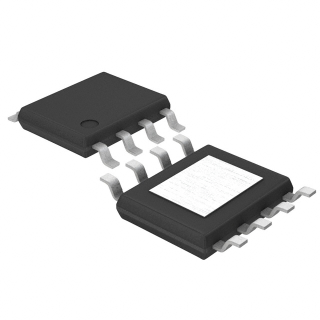
BD25GC0VEFJ-ME2
Active1A 2.5V, FIXED OUTPUT, HIGH-ACCURACY LDO REGULATOR FOR AUTOMOTIVE
Deep-Dive with AI
Search across all available documentation for this part.

BD25GC0VEFJ-ME2
Active1A 2.5V, FIXED OUTPUT, HIGH-ACCURACY LDO REGULATOR FOR AUTOMOTIVE
Deep-Dive with AI
Technical Specifications
Parameters and characteristics for this part
| Specification | BD25GC0VEFJ-ME2 |
|---|---|
| Control Features | Soft Start, Enable |
| Current - Output | 1 A |
| Current - Quiescent (Iq) | 1.2 mA |
| Grade | Automotive |
| Mounting Type | Surface Mount |
| Number of Regulators | 1 |
| Operating Temperature [Max] | 105 ░C |
| Operating Temperature [Min] | -40 °C |
| Output Configuration | Positive |
| Output Type | 1.81 mOhm |
| Package / Case | 0.154 in |
| Package / Case | 8-SOIC |
| Package / Case | 3.9 mm |
| Protection Features | Over Temperature, Over Current, Short Circuit |
| Qualification | AEC-Q100 |
| Supplier Device Package | 8-HTSOP-J |
| Voltage - Input (Max) [Max] | 14 V |
| Voltage - Output (Min/Fixed) | 2.5 V |
| Voltage Dropout (Max) [Max] | 1.2 V |
Pricing
Prices provided here are for design reference only. For realtime values and availability, please visit the distributors directly
| Distributor | Package | Quantity | $ | |
|---|---|---|---|---|
| Digikey | Cut Tape (CT) | 1 | $ 1.13 | |
| 10 | $ 0.82 | |||
| 25 | $ 0.74 | |||
| 100 | $ 0.65 | |||
| 250 | $ 0.61 | |||
| 500 | $ 0.59 | |||
| 1000 | $ 0.57 | |||
| Digi-Reel® | 1 | $ 1.13 | ||
| 10 | $ 0.82 | |||
| 25 | $ 0.74 | |||
| 100 | $ 0.65 | |||
| 250 | $ 0.61 | |||
| 500 | $ 0.59 | |||
| 1000 | $ 0.57 | |||
| Tape & Reel (TR) | 2500 | $ 0.55 | ||
| 5000 | $ 0.53 | |||
| 7500 | $ 0.53 | |||
| 12500 | $ 0.52 | |||
| 17500 | $ 0.51 | |||
| Newark | Each (Supplied on Cut Tape) | 1 | $ 2.03 | |
| 10 | $ 1.28 | |||
| 25 | $ 1.08 | |||
| 50 | $ 0.96 | |||
| 100 | $ 0.85 | |||
| 250 | $ 0.73 | |||
| 500 | $ 0.67 | |||
| 1000 | $ 0.55 | |||
Description
General part information
BD25GC0VEFJ-M Series
BDxxGC0VEFJ-M is a LDO regulator with output current 1.0A. The output accuracy is ±1% of output voltage. With external resistance, it is available to set the output voltage at random (from 1.5V to 13.0V).It has package type: HTSOP-J8. Overcurrent protection (for protecting the IC destruction by output short circuit), circuit current ON/OFF switch (for setting the circuit 0µA at shutdown mode), and thermal shutdown circuit (for protecting IC from heat destruction by over load condition)are all built in. It is usable for ceramic capacitor and enables to improve smaller set and long-life.This IC uses different production line against series model BD25GC0VEFJ-M for the purpose of improving production efficiency. We recommend using this IC for your new development. Electric characteristics noted in Datasheet does not differ between Production Line. In addition, the data of BD25GC0VEFJ-M is disclosed for documents and design models unless otherwise specified.
Documents
Technical documentation and resources


