LTC3589HUJ-1#PBF
Active8-OUTPUT REGULATOR WITH SEQUENCING AND I2C
Deep-Dive with AI
Search across all available documentation for this part.
LTC3589HUJ-1#PBF
Active8-OUTPUT REGULATOR WITH SEQUENCING AND I2C
Deep-Dive with AI
Technical Specifications
Parameters and characteristics for this part
| Specification | LTC3589HUJ-1#PBF |
|---|---|
| Applications | Handheld/Mobile Devices, OMAP™ |
| Current - Supply | 8 µA |
| Mounting Type | Surface Mount |
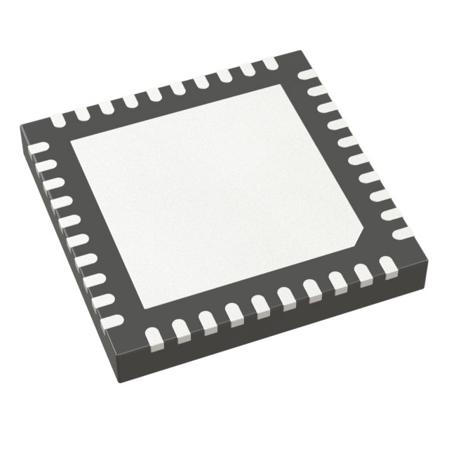
| Package / Case | 40-WFQFN Exposed Pad |
| Supplier Device Package | 40-QFN (6x6) |
| Voltage - Supply [Max] | 5.5 V |
| Voltage - Supply [Min] | 2.7 V |
Pricing
Prices provided here are for design reference only. For realtime values and availability, please visit the distributors directly
| Distributor | Package | Quantity | $ | |
|---|---|---|---|---|
| Digikey | Tube | 1 | $ 16.93 | |
| 10 | $ 12.18 | |||
| 25 | $ 10.95 | |||
| 61 | $ 8.90 | |||
| 100 | $ 9.59 | |||
| 122 | $ 8.47 | |||
| 250 | $ 8.93 | |||
| 500 | $ 8.52 | |||
| 1000 | $ 8.47 | |||
Description
General part information
LTC3589LTC3589-1LTC3589-2 Series
The LTC3589 is a complete power management solution for ARM and ARM-based processors and advanced portable microprocessor systems. The device contains three step-down DC/DC converters for core, memory and SoC rails, a buck-boost regulator for I/O at 1.8V to 5V and three 250mA LDO regulators for low noise analog supplies. An I2C serial port is used to control enables, output voltage levels, dynamic voltage scaling, operating modes and status reporting. Differences between the LTC3589, LTC3589-1, and LTC3589-2 are summarized in Table 1.Regulator start-up is sequenced by connecting outputs to enable pins in the desired order or programmed via the I2C port. System power-on, power-off, and reset functions are controlled by pushbutton interface, pin inputs, or I2C interface.The LTC3589 supports i.MX53/51, PXA and OMAP processors with eight independent rails at appropriate power levels. Other features include interface signals such as the VSTB pin that simultaneously toggle up to four rails between programmed run and standby output voltages. The device is available in a low profile 40-pin 6mm × 6mm exposed pad QFN package.LTC3589LTC3589-1LTC3589-2Power-On Inhibit Enable Delay1 second2ms2msBuck 2 & 3 Current Output1A1.2A1.2APGOOD Fault TimeoutEnabled Default, I2C DisableDisabled by Default, I2C EnableDisabled by Default, I2C EnablePWR_ON to WAKE Delay50ms2ms2msLDO3 Vout1.8V2.8V2.8VLDO4 Vout1.8V, 2.5V, 2.8V, 3.3V1.2V, 1.8V, 2.5V, 3.2V1.2V, 1.8V, 2.5V, 3.2VLDO4 Vout1.8V, 2.5V, 2.8V, 3.3V1.2V, 1.8V, 2.5V, 3.2V1.2V, 1.8V, 2.5V, 3.2VDefault LDO4 EnableLDO34_EN (Pin) or I2CI2C OnlyI2C OnlyWait to Enable Until Output < 300mVYes. Change with I2CYes. Change with I2CNo. Change with I2CInsert 2.5K Discharge Resistor When DisabledYes when Wait to Enable Until Output < 300mVYes when Wait to Enable Until Output < 300mVAlways inserted when regulator disabledApplicationsHandheld Instruments and ScannersPortable Industrial DevicesAutomotive InfotainmentMedical DevicesHigh End Consumer DevicesMultirail SystemsSupports Freescale i.MX53/51, Marvell PXA and Other Application Processors
Documents
Technical documentation and resources