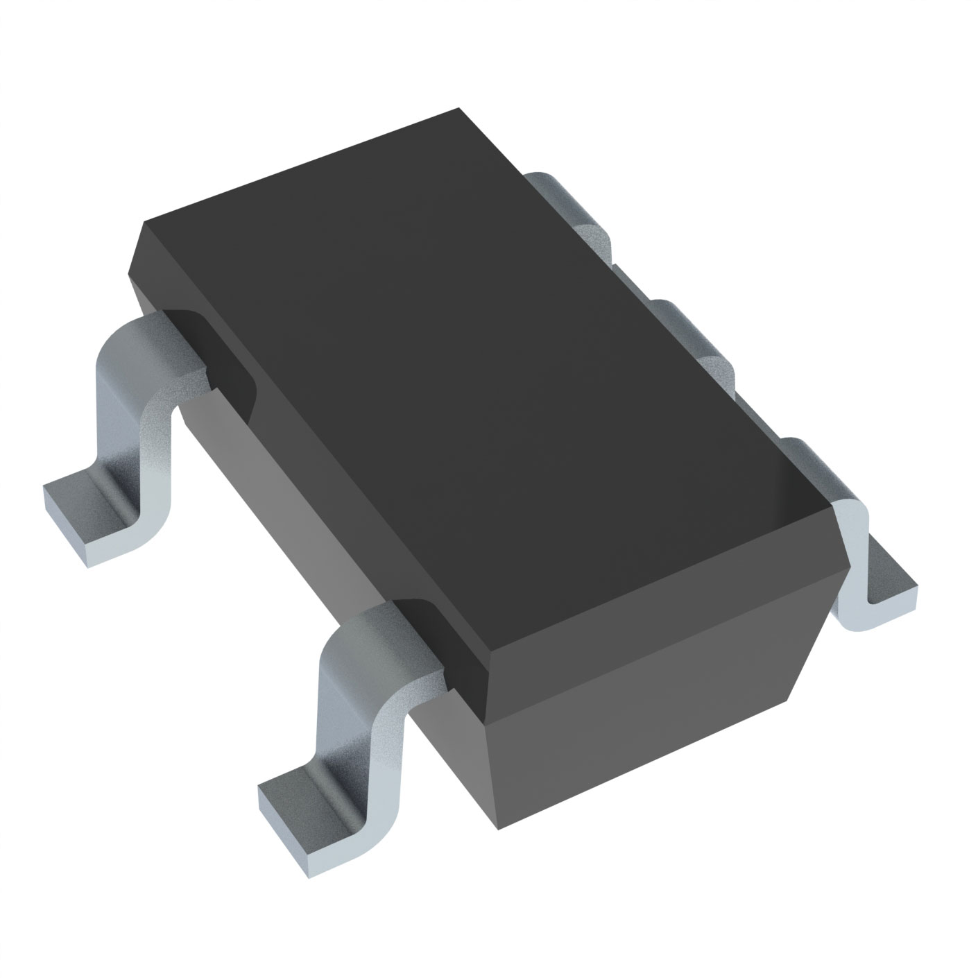
UCC27519DBVT
Active4-A/4-A SINGLE-CHANNEL GATE DRIVER WITH 5-V UVLO, ENABLE, AND CMOS INPUT
Deep-Dive with AI
Search across all available documentation for this part.

UCC27519DBVT
Active4-A/4-A SINGLE-CHANNEL GATE DRIVER WITH 5-V UVLO, ENABLE, AND CMOS INPUT
Technical Specifications
Parameters and characteristics for this part
| Specification | UCC27519DBVT |
|---|---|
| Channel Type | Single |
| Current - Peak Output (Source, Sink) [custom] | 4 A |
| Current - Peak Output (Source, Sink) [custom] | 4 A |
| Driven Configuration | Low-Side |
| Gate Type | N-Channel MOSFET, IGBT |
| Input Type | Non-Inverting |
| Mounting Type | Surface Mount |
| Number of Drivers | 1 |
| Operating Temperature [Max] | 140 °C |
| Operating Temperature [Min] | -40 °C |
| Package / Case | SC-74A, SOT-753 |
| Rise / Fall Time (Typ) [custom] | 7 ns |
| Rise / Fall Time (Typ) [custom] | 8 ns |
| Supplier Device Package | SOT-23-5 |
| Voltage - Supply [Max] | 18 V |
| Voltage - Supply [Min] | 4.5 V |
Pricing
Prices provided here are for design reference only. For realtime values and availability, please visit the distributors directly
| Distributor | Package | Quantity | $ | |
|---|---|---|---|---|
| Digikey | Cut Tape (CT) | 1 | $ 1.10 | |
| 10 | $ 0.98 | |||
| 25 | $ 0.93 | |||
| 100 | $ 0.77 | |||
| Digi-Reel® | 1 | $ 1.10 | ||
| 10 | $ 0.98 | |||
| 25 | $ 0.93 | |||
| 100 | $ 0.77 | |||
| Tape & Reel (TR) | 250 | $ 0.72 | ||
| 500 | $ 0.63 | |||
| 1250 | $ 0.50 | |||
| 2500 | $ 0.47 | |||
| 6250 | $ 0.44 | |||
| 12500 | $ 0.43 | |||
| LCSC | Piece | 1 | $ 0.93 | |
| 10 | $ 0.76 | |||
| 30 | $ 0.67 | |||
| 250 | $ 0.55 | |||
| 500 | $ 0.50 | |||
| 1000 | $ 0.47 | |||
| Texas Instruments | SMALL T&R | 1 | $ 0.81 | |
| 100 | $ 0.63 | |||
| 250 | $ 0.46 | |||
| 1000 | $ 0.33 | |||
Description
General part information
UCC27519 Series
The UCC27518 and UCC27519 single-channel, high-speed, low-side gate driver device can effectively drive MOSFET and IGBT power switches. Using a design that inherently minimizes shoot-through current, UCC27518 and UCC27519 can source and sink high, peak-current pulses into capacitive loads offering rail-to-rail drive capability and extremely small propagation delay typically 17 ns.
The UCC27518 and UCC27519 provide 4-A source, 4-A sink (symmetrical drive) peak-drive current capability at VDD = 12 V.
The UCC27518 and UCC27519 are designed to operate over a wide VDD range of 4.5 V to 18 V and a wide temperature range of –40°C to 140°C. Internal under voltage lockout (UVLO) circuitry on the VDD pin holds output low outside VDD operating range. The capability to operate at low voltage levels such as below 5 V, along with best-in-class switching characteristics, is especially suited for driving emerging wide band-gap power switching devices such as GaN power semiconductor devices.
Documents
Technical documentation and resources


