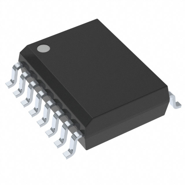
UCC20520DW
LTB5.7-KVRMS, 4-A/6-A DUAL-CHANNEL ISOLATED GATE DRIVER WITH SINGLE INPUT, 8-V UVLO & LGA PACKAGE
Deep-Dive with AI
Search across all available documentation for this part.

UCC20520DW
LTB5.7-KVRMS, 4-A/6-A DUAL-CHANNEL ISOLATED GATE DRIVER WITH SINGLE INPUT, 8-V UVLO & LGA PACKAGE
Technical Specifications
Parameters and characteristics for this part
| Specification | UCC20520DW |
|---|---|
| Approval Agency | CQC, CSA, VDE, UR |
| Common Mode Transient Immunity (Min) [Min] | 100 V/ns |
| Current - Output High, Low | 4 A, 6 A |
| Mounting Type | Surface Mount |
| Number of Channels [custom] | 2 |
| Operating Temperature [Max] | 125 °C |
| Operating Temperature [Min] | -40 °C |
| Package / Case | 16-SOIC |
| Package / Case [x] | 0.295 in |
| Package / Case [y] | 7.5 mm |
| Propagation Delay tpLH / tpHL (Max) [Max] | 30 ns |
| Pulse Width Distortion (Max) | 5 ns |
| Rise / Fall Time (Typ) [custom] | 7 ns |
| Rise / Fall Time (Typ) [custom] | 6 ns |
| Supplier Device Package | 16-SOIC |
| Technology | Capacitive Coupling |
| Voltage - Isolation | 5700 Vrms |
| Voltage - Output Supply [Max] | 25 V |
| Voltage - Output Supply [Min] | 9.2 V |
Pricing
Prices provided here are for design reference only. For realtime values and availability, please visit the distributors directly
| Distributor | Package | Quantity | $ | |
|---|---|---|---|---|
| Digikey | Tube | 1 | $ 7.51 | |
| 10 | $ 5.13 | |||
| 25 | $ 4.51 | |||
| 100 | $ 3.82 | |||
| 250 | $ 3.49 | |||
| 500 | $ 3.28 | |||
| 1000 | $ 3.11 | |||
| Texas Instruments | TUBE | 1 | $ 5.27 | |
| 100 | $ 4.62 | |||
| 250 | $ 3.24 | |||
| 1000 | $ 2.61 | |||
Description
General part information
UCC20520 Series
The UCC20520 is an isolated single input, dual-channel gate driver with 4-A source and 6-A sink peak current. It is designed to drive power MOSFETs, IGBTs, and SiC MOSFETs up to 5-MHz with best-in-class propagation delay and pulse-width distortion.
The input side is isolated from the two output drivers by a 5.7-kVRMSreinforced isolation barrier, with a minimum of 100-V/ns common-mode transient immunity (CMTI). Internal functional isolation between the two secondary-side drivers allows a working voltage of up to 1500-VDC.
This driver can be used for half-bridge driver with programmable dead time (DT). A disable pin shuts down both outputs simultaneously when it is set high, and allows normal operation when left open or grounded. As a fail-safe measure, primary-side logic failures force both outputs low.
Documents
Technical documentation and resources


