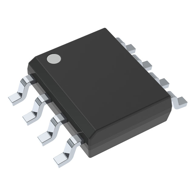
UC2572DG4
UnknownIC REG CTRLR FLYBACK 8SOIC
Deep-Dive with AI
Search across all available documentation for this part.

UC2572DG4
UnknownIC REG CTRLR FLYBACK 8SOIC
Deep-Dive with AI
Technical Specifications
Parameters and characteristics for this part
| Specification | UC2572DG4 |
|---|---|
| Clock Sync | False |
| Control Features | Ramp, Current Limit |
| Duty Cycle (Max) [Max] | 92 % |
| Frequency - Switching | 100 kHz |
| Function | Step-Up/Step-Down |
| Mounting Type | Surface Mount |
| Number of Outputs | 1 |
| Operating Temperature [Max] | 85 °C |
| Operating Temperature [Min] | -40 °C |
| Output Configuration | Negative |
| Output Phases | 1 |
| Output Type | Transistor Driver |
| Package / Case | 8-SOIC |
| Package / Case [x] | 0.154 in |
| Package / Case [y] | 3.9 mm |
| Supplier Device Package | 8-SOIC |
| Synchronous Rectifier | False |
| Topology | Flyback |
| Voltage - Supply (Vcc/Vdd) [Max] | 30 V |
| Voltage - Supply (Vcc/Vdd) [Min] | 4.75 V |
UC2572 Series
Negative output Flyback pulse width modulator
| Part | Mounting Type | Package / Case | Package / Case [y] | Package / Case [x] | Output Phases | Function | Output Configuration | Control Features | Output Type | Voltage - Supply (Vcc/Vdd) [Max] | Voltage - Supply (Vcc/Vdd) [Min] | Number of Outputs | Supplier Device Package | Duty Cycle (Max) [Max] | Topology | Operating Temperature [Max] | Operating Temperature [Min] | Frequency - Switching | Synchronous Rectifier | Clock Sync | Package / Case | Package / Case |
|---|---|---|---|---|---|---|---|---|---|---|---|---|---|---|---|---|---|---|---|---|---|---|
Texas Instruments | Surface Mount | 8-SOIC | 3.9 mm | 0.154 in | 1 | Step-Up/Step-Down | Negative | Current Limit Ramp | Transistor Driver | 30 V | 4.75 V | 1 | 8-SOIC | 92 % | Flyback | 85 °C | -40 °C | 100 kHz | ||||
Texas Instruments | Surface Mount | 8-SOIC | 3.9 mm | 0.154 in | 1 | Step-Up/Step-Down | Negative | Current Limit Ramp | Transistor Driver | 30 V | 4.75 V | 1 | 8-SOIC | 92 % | Flyback | 85 °C | -40 °C | 100 kHz | ||||
Texas Instruments | Through Hole | 8-DIP | 1 | Step-Up/Step-Down | Negative | Current Limit Ramp | Transistor Driver | 30 V | 4.75 V | 1 | 8-PDIP | 92 % | Flyback | 85 °C | -40 °C | 100 kHz | 0.3 in | 7.62 mm |
Pricing
Prices provided here are for design reference only. For realtime values and availability, please visit the distributors directly
| Distributor | Package | Quantity | $ | |
|---|---|---|---|---|
| Digikey | Tube | 225 | $ 3.11 | |
Description
General part information
UC2572 Series
The UC3572 is a negative output flyback pulse width modulator which converts a positive input voltage to a regulated negative output voltage. The chip is optimized for use in a single inductor negative flyback switching converter employing an external PMOS switch. The block diagram consists of a precision reference, an error amplifier configured for voltage mode operation, an oscillator, a PWM comparator with latching logic, and a 0.5A peak gate driver. The UC3572 includes an undervoltage lockout circuit to insure sufficient input supply voltage is present before any switching activity can occur, and a pulse-by-pulse current limit. Output current can be sensed and limited to a user determined maximum value. The UVLO circuit turns the chip off when the input voltage is below the UVLO threshold. In addition, a sleep comparator interfaces to the UVLO circuit to turn the chip off. This reduces the supply current to only 50uA, making the UC3572 ideal for battery powered applications.
The UC3572 is a negative output flyback pulse width modulator which converts a positive input voltage to a regulated negative output voltage. The chip is optimized for use in a single inductor negative flyback switching converter employing an external PMOS switch. The block diagram consists of a precision reference, an error amplifier configured for voltage mode operation, an oscillator, a PWM comparator with latching logic, and a 0.5A peak gate driver. The UC3572 includes an undervoltage lockout circuit to insure sufficient input supply voltage is present before any switching activity can occur, and a pulse-by-pulse current limit. Output current can be sensed and limited to a user determined maximum value. The UVLO circuit turns the chip off when the input voltage is below the UVLO threshold. In addition, a sleep comparator interfaces to the UVLO circuit to turn the chip off. This reduces the supply current to only 50uA, making the UC3572 ideal for battery powered applications.
Documents
Technical documentation and resources


